ContentsFigures & Tables
In recent years, two-dimensional (2D) magnetic materials have garnered significant attention due to their exceptional electronic, magnetic, and optical properties, making them promising candidates for advancing nanoelectronic and spintronic technologies [1–8]. Among these materials, CrSBr stands out as a unique quasi-2D semiconductor, distinguished by its layered structure and intrinsic magnetic order [9–14]. The interplay between CrSBr's electronic structure, surface properties, and external variables—such as temperature and thickness—provides a versatile platform for both fundamental research and technological innovation.
The work function, defined as the minimum energy required to extract an electron from a material's surface into a vacuum, plays a pivotal role in determining its electronic and optoelectronic behavior [15–18]. In 2D materials, the work function is highly sensitive to intrinsic factors, such as thickness, quantum confinement, and interlayer coupling, as well as extrinsic factors, including temperature, strain, and substrate interactions [19–22]. Notably, recent studies on other 2D ferromagnetic semiconductors—such as CrI3 [23], Cr2Ge2Te6 [24, 25], and Fe3GeTe2 [26] —have demonstrated that their work functions typically range from 4 to 6 eV and vary significantly with thickness and interface conditions, highlighting the critical role of electronic structure modulation in low-dimensional magnetic systems. Consequently, a comprehensive understanding and precise modulation of the work function in CrSBr are essential for optimizing its performance in applications such as sensors, transistors, and thermally stable electronic devices [27–29]. Despite notable advancements in elucidating the physical properties of CrSBr, the intricate relationship between its work function, material thickness, and temperature-dependent behavior remains insufficiently explored. Previous studies have often overlooked the complex interplay between surface states, layer-dependent electronic structures, and thermally induced carrier dynamics—factors critical in shaping low-dimensional materials' work function.
This work synthesized high-quality CrSBr single crystals via the chemical vapor transport (CVT) method. The surface work function of CrSBr was systematically investigated as a function of thickness and temperature using scanning Kelvin probe microscopy (SKPM), revealing a nonlinear dependence on thickness and a tunable, reversible behavior with respect to temperature. The influence of work function modulation on charge injection was further validated through a 2D field-effect transistor (FET), demonstrating temperature-induced variation in Schottky barrier height. In addition, first-principles calculations elucidated the effects of layer number and magnetic configuration on the work function of few-layer CrSBr. Together, these results establish a solid foundation for applying CrSBr in photothermal sensing, spintronic devices, and van der Waals electronic systems.
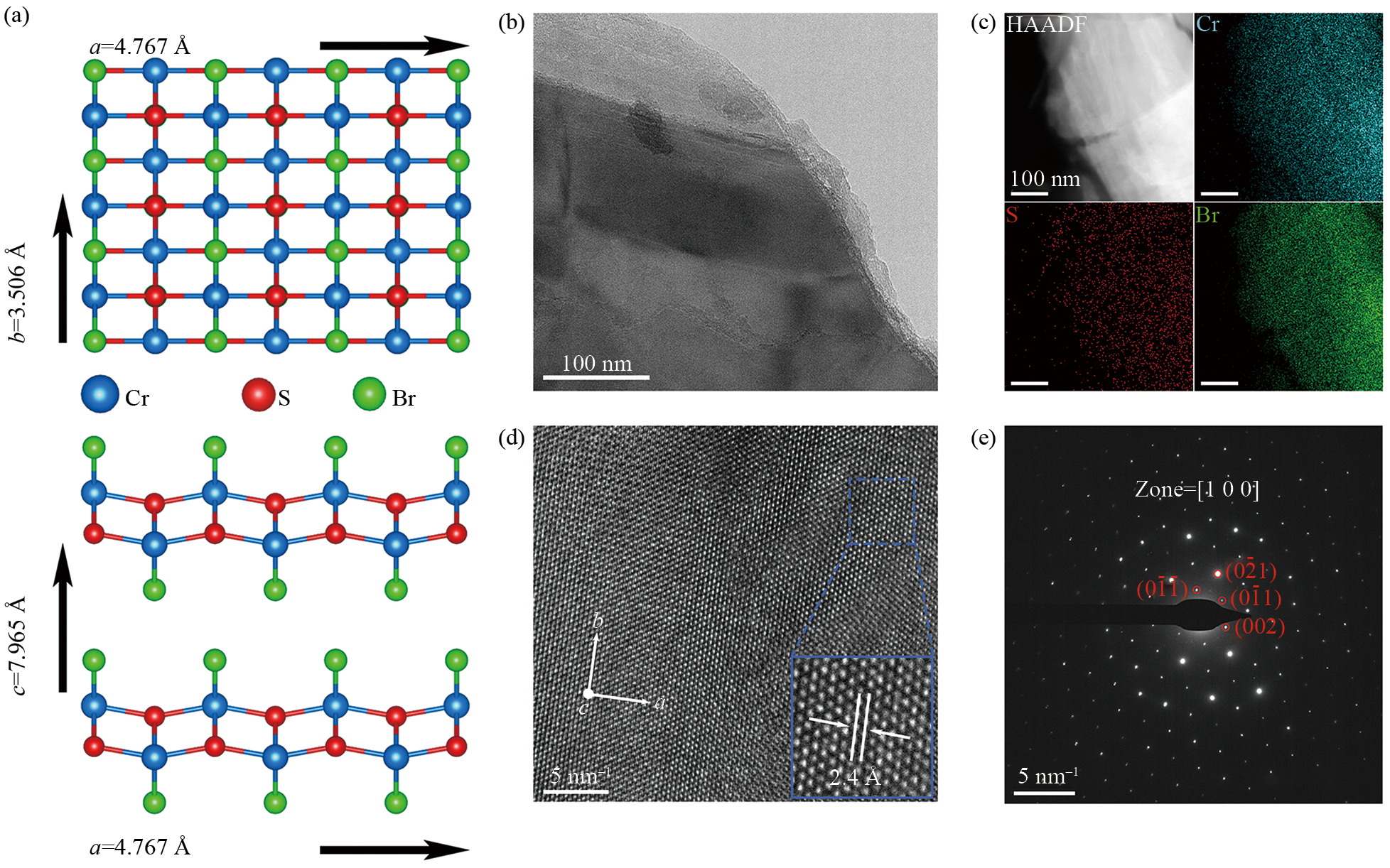
The morphology and structure of the exfoliated few-layer CrSBr were characterized using transmission electron microscopy (TEM). Figure 1(a) shows both in-plane and out-of-plane views of the atomic lattice, confirming the layered structure of CrSBr with lattice constants a=4.767 Å, b=3.506 Å, and c=7.965 Å. Figure 1(b) displays a low-magnification TEM image of the CrSBr with a distinct thin layered structure. High-angle annular dark-field scanning TEM (HAADF-STEM) and energy dispersive spectroscopy (EDS) images (Fig. 1(c)) confirm the presence and uniform distribution of Cr, S, and Br elements within the few-layer CrSBr. The high-magnification HAADF-STEM image (Fig. 1(d)) reveals a well-ordered lattice structure, with a spacing of 4.8 Å between adjacent S/Br atoms along the a-axis. The selected area electron diffraction (SAED) pattern (Fig. 1(e)) along the [100] zone axis exhibits characteristic diffraction spots of the orthorhombic crystal structure, with clearly identifiable diffraction spots corresponding to the (002), (01), (01), and (0) crystal planes. These diffraction features align closely with the expected crystallographic characteristics of CrSBr, confirming the high crystalline quality of the material synthesized via the CVT method. Consequently, the TEM characterization results robustly demonstrate the high-quality crystal structure of the prepared sample, providing a reliable structural foundation for further research.
We characterized the exfoliated layered CrSBr using photoluminescence (PL) and Raman spectroscopy. The optical morphology of the mechanically exfoliated CrSBr crystal is shown in Fig. 2(a). Figure 2(b) presents the corresponding PL spectrum, where a prominent emission peak is observed at 1.44 eV. The central emission peak exhibits a slight redshift with increasing thickness (Fig. S1), which is attributed to quantum confinement effects and the weakened interlayer coupling in thinner flakes [30, 31]. This peak value corresponds to the bandgap energy of CrSBr [14, 32], indicating that CrSBr possesses semiconductor properties.
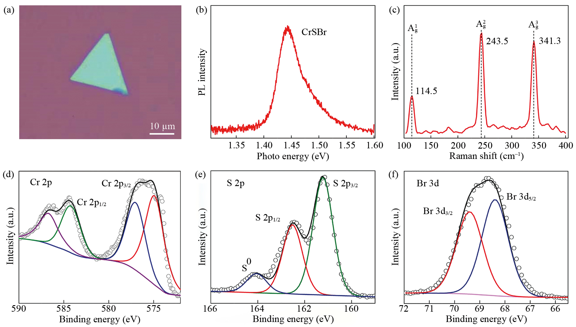
The Raman spectroscopy analysis was performed on the synthesized CrSBr crystals to explore their lattice vibration characteristics. As presented in Fig. 1, CrSBr has an orthorhombic crystal structure, belonging to the Pmmn space group. Each monolayer consists of two layers of chromium (Cr) and sulfur (S) atoms with bromine (Br) atoms sandwiched in between [32]. The bromine atoms are positioned at the top and bottom of each monolayer, while the sulfur and chromium atoms are in the middle. Therefore, in few-layer CrSBr, the bromine atoms primarily mediate interlayer vibrational coupling. Figure 2(c) presents the Raman spectrum of CrSBr, showing three distinct Raman-active modes at 114.5, 243.5, and 341.3 cm⁻¹. These peaks correspond to different lattice vibration modes in CrSBr, specifically the , , and modes, respectively. The mode mainly involves the vibrations of Cr and Br atoms perpendicular to the layer plane. The relatively low intensity of this peak suggests a small Raman scattering cross-section for this vibration mode. The mode is related to the in-plane vibrations of Cr atoms, and this peak has the highest intensity, possibly because the in-plane movement of Cr atoms is more responsive to the incident light. The mode involves the cooperative vibrations of Cr and S atoms within the layers. The high intensity of this peak may be due to the critical role of the cooperative vibrations of Cr and S atoms in the structure, indicating a higher contribution from bromine and thus higher interlayer coupling [33]. These results suggest that CrSBr has semiconductor characteristics [34], consistent with our expectations of the CrSBr crystal structure and further confirming its orthorhombic crystal structure and interlayer coupling characteristics.
At room temperature, the X-ray photoelectron spectroscopy (XPS) survey spectrum of the CrSBr crystal clearly revealed the presence of Cr, S, and Br elements (Fig. S2). Deconvolution of the high-resolution XPS spectra showed that the Cr 3d orbitals (2p3/2 and 2p1/2) were located at 574.9 eV and 584.2 eV, respectively; the S 2p orbitals (2p3/2 and 2p1/2) were positioned at 161.2 eV and 162.5 eV; and the Br 3d orbitals (3d5/2 and 3d3/2) appeared at 68.3 eV and 69.4 eV, respectively. These results are consistent with previously reported literature [9, 35] and further confirm the presence of Cr3+, S2–, and Br⁻ ions in the synthesized sample, forming S-Cr-Br chemical bonds, thereby indicating the high crystalline quality of the material.
In conclusion, the comprehensive analysis using PL, Raman spectroscopy, and XPS has conclusively demonstrated that CrSBr crystals synthesized via the CVT method possess excellent crystalline quality. These crystals can be effectively exfoliated into few-layer nanosheets and exhibit a well-defined semiconductor bandgap.
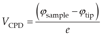
In this study, we investigated the potential correlation between the work function and thickness of CrSBr nanosheets using a SKPM system (Figs. 3(a)–3(f)). The nanosheet samples were exfoliated using specialized adhesive tape and transferred onto a gold-coated silicon substrate. To ensure measurement accuracy, highly oriented pyrolytic graphite (HOPG) was used as a reference sample for calibrating the probe work function, which was determined to be 4.58 eV post-calibration. Subsequently, the corresponding sample work function was obtained using the equation:(1)Where VCPD is the contact potential difference, and e is the elementary charge.
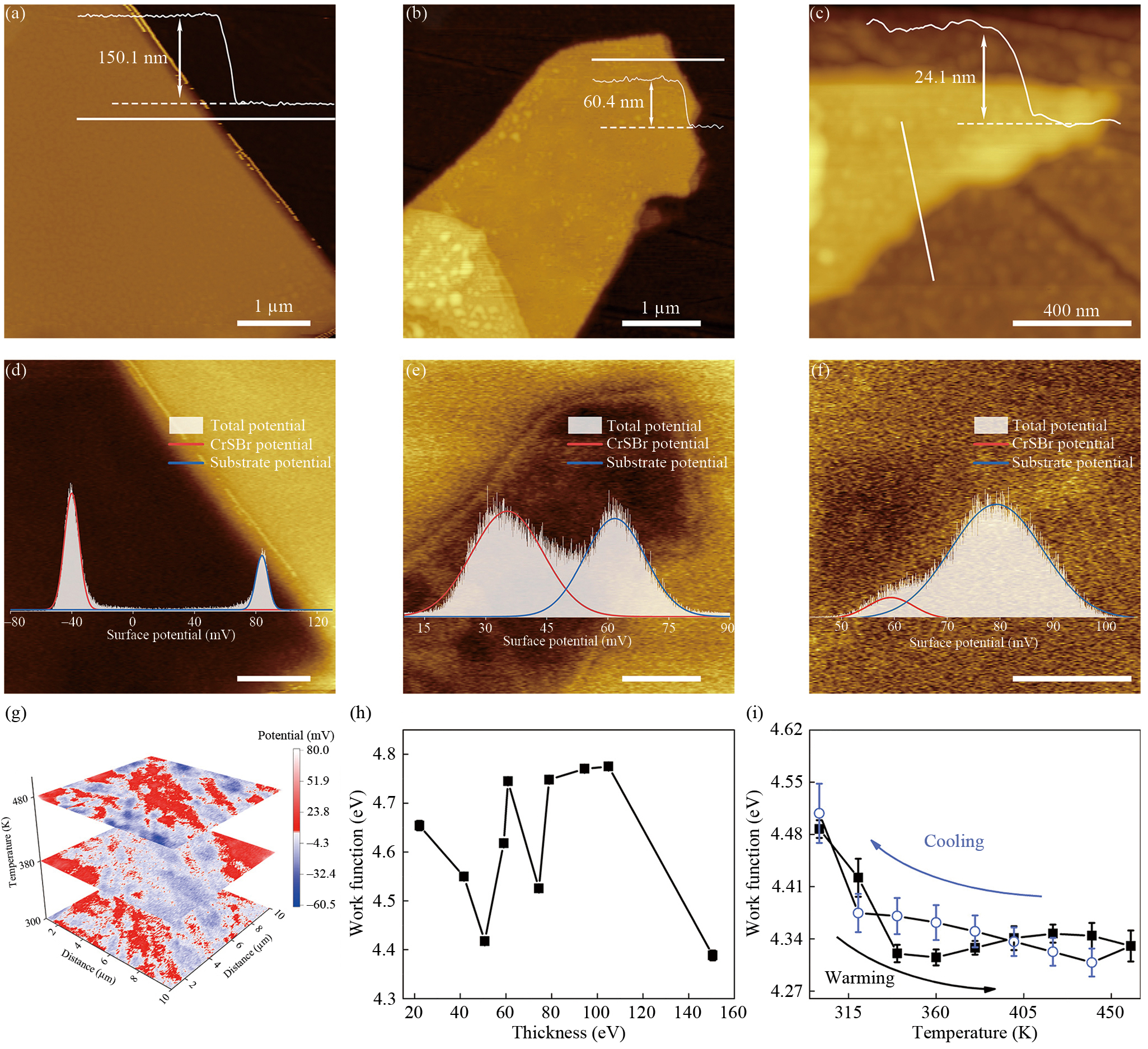
Figures 3(a) and 3(b) demonstrate a significant surface potential difference of 123.9 mV between the CrSBr nanosheet (with a thickness of 150.1 nm) and the substrate. As the thickness decreased, the surface potential difference diminished, reaching 26.3 mV at 60.4 nm and 20.3 mV at 24.1 nm. This trend can be attributed to the reduction in overall charge screening effects as the material becomes thinner. This leads to more uniform charge distribution and stronger coupling between the substrate and the material, thereby reducing the surface-substrate potential difference. However, statistical analysis of the work function for CrSBr samples of varying thicknesses (Fig. 3(h)) reveals no clear linear relationship between the work function and thickness. This nonlinearity may result from irregularities induced by surface states and van der Waals interactions [36, 37]. Additionally, quantum confinement effects [38, 39] may also play a significant role. These interactions induce complex modulations in the work function, resulting in a non-linear dependence of the CrSBr work function on thickness.
To directly modulate the work function of CrSBr nanosheets, we investigated the surface potential variation of CrSBr under different temperatures. To minimize the influence of substrate coupling, the measurements were conducted on a CrSBr bulk sample with a thickness of 1.3 μm, as depicted in Fig. S3. Figure 3(g) illustrates the surface potential distribution at 300, 380, and 480 K. The results show a significant change in surface potential at 380 K, while at 480 K, the potential distribution returns to a state similar to that observed at 300 K. This indicates that thermal excitation induces carrier migration within the material until the local carrier concentration reaches saturation, stabilizing the thermal excitation effect and restoring the surface potential distribution to its initial state [40, 41]. Figure 3(i) depicts the variation in the work function of CrSBr as a function of temperature. As the temperature increases, the work function initially decreases, stabilizing after reaching 360 K. During cooling, the work function gradually increases with decreasing temperature, exhibiting a more pronounced change at 340 K. This behavior can be attributed to thermal excitation, which facilitates the transition of more electrons into the conduction band at elevated temperatures, thereby increasing surface electron density. Consequently, electrons are more readily excited out of the material, reducing the work function. As the temperature rises, the concentration of thermally excited carriers saturates, causing the surface charge distribution to stabilize and the work function to plateau. Throughout the entire temperature cycle, the work function exhibits a consistent trend, demonstrating the reversible nature of CrSBr in response to temperature variations. This further confirms that, after thermal cycling, the material's surface charge distribution and band structure can return to their original state without irreversible structural changes or chemical reactions. Thus, CrSBr exhibits excellent thermal stability and stable surface characteristics within a certain temperature range.
To further investigate the tunability of the work function in few-layer CrSBr, we performed systematic calculations based on density functional theory (DFT). We first analyzed the projected density of states (PDOS) of a few-layer CrSBr under both ferromagnetic (FM) and antiferromagnetic (AFM) spin configurations (Fig. S4). The results indicate that few-layer CrSBr is a narrow-bandgap semiconductor. In the AFM configuration (Figs. S4(a)–S4(d)), the bandgap decreases progressively with increasing layer number, which can be attributed to the reduced quantum confinement effect as the system size increases. Notably, in the FM configuration (Figs. S4(e)–S4(h)), both the conduction band minimum and valence band maximum are located in the same spin-up channel, giving rise to a narrow direct bandgap, while the spin-down channel exhibits a much wider gap, indicating a strong spin polarization. Additionally, a significant overlap between the Cr d orbitals and S/Br p orbitals is observed in the energy bands, revealing pronounced d–p hybridization. This suggests the presence of superexchange interactions mediated by p orbitals between neighboring Cr atoms via S/Br atoms, which is consistent with previous reports on CrSBr [42].
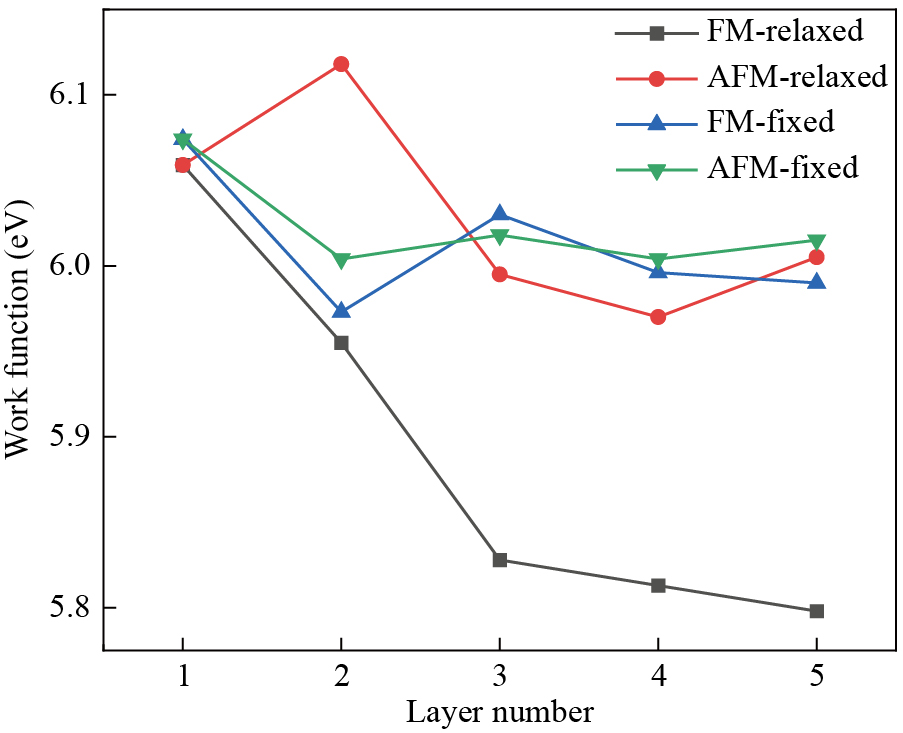
For work function calculations, we define the work function as the energy difference between the vacuum level and the Fermi level. We further evaluated the layer- and magnetism-dependent evolution of the work function, considering four configurations: FM-relaxed and AFM-relaxed (structures optimized under respective spin configurations), and FM-fixed and AFM-fixed (spin configurations imposed on pre-optimized structures) (Fig. 4). The results show that the work function of CrSBr is highly sensitive to both the number of layers and the magnetic ordering. It decreases rapidly with increasing layer number and saturates beyond three layers, which aligns well with the bandgap narrowing trend observed in PDOS, indicating that the shift of the Fermi level toward the vacuum level is the dominant factor driving the reduction in work function. Furthermore, in both FM and AFM configurations, magnetic ordering results in a significantly lower work function than the nonmagnetic counterparts, underscoring the crucial role of magnetism in modulating surface electronic properties.
In summary, first-principles calculations demonstrate that few-layer CrSBr exhibits excellent work function tunability governed by both layer thickness and magnetic order, providing theoretical guidance for its potential applications in spintronic devices and multifunctional field-effect transistors.
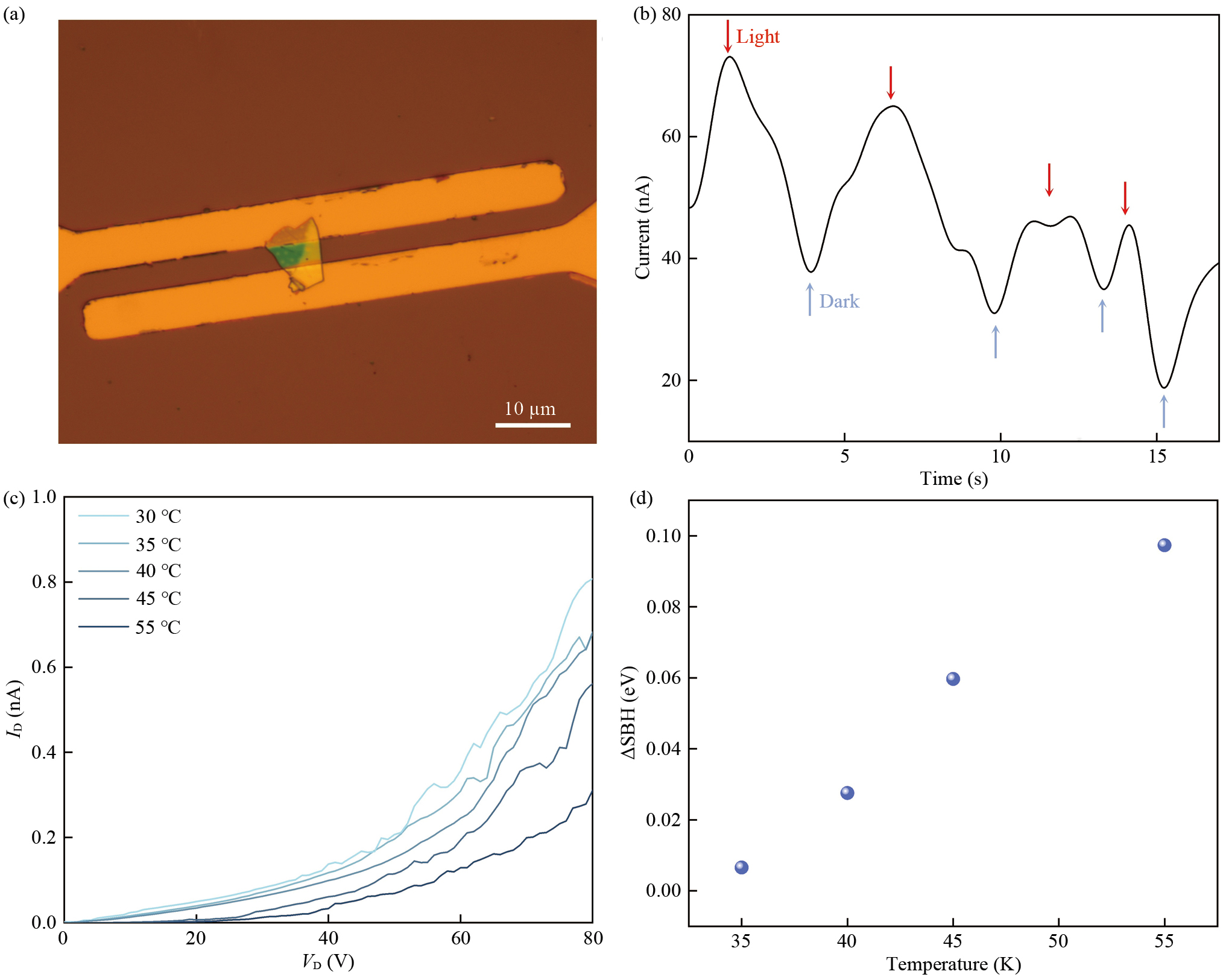
As a practical demonstration, a CrSBr-based FET was fabricated to examine the role of work function modulation in 2D semiconductors (Fig. 5(a)). Under light illumination, the device exhibited a significant increase in drain current (Fig. 5(b)), indicating the participation of photogenerated carriers in conduction. This observation confirms that CrSBr possesses a finite bandgap and exhibits typical semiconducting behavior. The output characteristics of the CrSBr FET at different temperatures are shown in Fig. 5(c). At a fixed gate voltage of 3 V, the drain current gradually decreases with increasing temperature, suggesting that temperature has a pronounced effect on carrier injection at the metal–semiconductor interface.
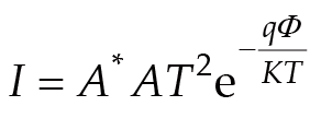
According to the classical Schottky barrier current model [43, 44], the reverse saturation current I is related to the Schottky barrier height Φ via the following expression:(2)
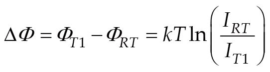
Here, I represents the reverse saturation current, which can be extracted from the linear extrapolation of the output characteristics in the low-bias region. Based on Eq. (2), the relative change in barrier height under different temperature conditions can be derived as:(3)
Using this relation, the change in Schottky barrier height (SBH) with respect to that at 30 °C was calculated and is presented in Fig. 5(d), with values of 0.007 eV, 0.028 eV, 0.060, and 0.097 eV, respectively. This trend is consistent with the temperature-dependent decrease in the CrSBr work function observed in the SKPM measurements (Fig. 3(i)), further verifying that work function modulation plays a key role in regulating carrier transport behavior.
These results strongly support the electronic nature of CrSBr as a two-dimensional n-type semiconductor and demonstrate the feasibility of temperature-responsive Schottky barrier modulation. This mechanism provides a solid physical foundation for the development of temperature-sensitive FETs, thermally tunable spintronic devices, and programmable photo-/thermal-responsive logic circuits, thereby expanding the potential of CrSBr in adaptive van der Waals device architectures.
In conclusion, this study comprehensively investigates the nonlinear relationship between the thickness of CrSBr nanosheets and their work function using SKPM. Importantly, the work function is thermally tunable, enabling effective modulation of the Schottky barrier height in CrSBr-based 2D FETs. Complementary first-principles calculations further uncover the work function's dependence on layer thickness and magnetic ordering. In addition, the experimental results demonstrate the excellent thermal stability of CrSBr. These findings establish a critical experimental foundation for the design and application of CrSBr in low-power devices, sensors, and spintronic devices.
High-purity Cr powder, sulfur powder, and CrBr3 were mixed in a molar ratio of 1.3∶3∶1.7, with CrBr3 serving as both the source of Br and the transport agent. The reaction was conducted in a sealed vacuum quartz ampoule, maintaining a 10–4 Pa pressure. A dual-zone tube furnace was used to control the reaction temperature. Initially, the temperature of the charge region and the sink region was raised from room temperature to 850 °C and 950 °C, respectively, over 24 hours. After maintaining these temperatures for 24 hours, the charge region was further heated to 950 °C while the sink region was cooled to 850 °C over 12 hours. The temperature was then held constant for 48 hours before cooling to room temperature over 6 hours, forming CrSBr crystals in the sink region. The crystals were subsequently soaked and washed sequentially using 1 mg/mL CrCl2 solution, deionized water, and acetone to remove by-products and impurities.
CrSBr crystals were exfoliated using the mechanical exfoliation method and transferred onto a 60 nm gold-coated silicon substrate. Conductive silver paste was applied to ground the substrate and sample, preventing charge accumulation. Surface potential information was collected using a conductive probe (NanoSensor, PPP-EFM) in Kelvin probe force microscopy mode (Cypher ES, Asylum Research). The work function of the probe was calibrated using highly oriented pyrolytic graphite (HOPG, manufacturer model), with the default work function of HOPG set to 4.6 eV.
First-principles calculations were carried out using the VASP code within the framework of DFT. The PAW method and PBE functional were employed, with a plane-wave cutoff energy of 500 eV and a 5×5×1 Γ-centered k-point mesh. Structural relaxations were performed until the forces were below 0.01 eV·Å–1. A 20 Å vacuum layer was applied to avoid interlayer interactions. Both FM and AFM configurations were considered for 2–5 layers of CrSBr. PDOS were computed to evaluate layer-dependent electronic properties.
Few-layer CrSBr nanosheets were mechanically exfoliated onto Si/SiO2 substrates (300 nm oxide). Source and drain electrodes (5 nm Cr / 50 nm Au) were patterned via electron-beam lithography and deposited by thermal evaporation. The heavily doped Si substrate served as the global back gate. Electrical and photoresponse measurements in atmospheric environments were performed using a semiconductor parameter analyzer under both dark and illuminated conditions. Temperature-dependent transport was measured from room temperature to 460 K using a probe station with a heating stage.
The authors acknowledge support from the National Key Research and Development Project (Grant No. 2024YFA1408802), the Key Research and Development Program of Shaanxi (Grant No. 2025GH-YBXM-050), the National Natural Science Foundation of China (Grant Nos. 12204294, 62304069, 52202186, and 12104352), the China National Postdoctoral Programme for Innovative Talents (No. BX20230281), the Natural Science Basic Research Program of Shaanxi (Program No. 2023JC-XJ-01), Ningxia Key Research and Development Program (Grant No. 2020BEB04042), Xidian University Specially Funded Project for Interdisciplinary Exploration (Nos. TZJH2024064 and TZJH2024053), the Fundamental Research Funds for the Central Universities, the Innovation Fund of Xidian University, and the China Postdoctoral Science Foundation (Certifcate No. 2024M752520). The numerical calculations in this paper were supported by the High-Performance Computing Platform of Xidian University.
Y. Wang, W. Xu, D. Yang, Y. Zhang, Y. Xu, Z. Cheng, X. Mi, Y. Wu, Y. Liu.et al, "Above-room-temperature strong ferromagnetism in 2D MnB nanosheet," ACS Nano, vol. 17, pp. 24320–24328, 2023.
Y. Xu, D. Yang, Y. Zhang, G. Yuan, Y. Zou, Z. Zhang, Y. Wang, and Y. Wu, "Realizing room-temperature ferromagnetism in metal-free graphene through vacancy-assisted hydrogenation," Chain, vol. 2, pp. 72–80, 2025.
Y. Wu, Y. Liu, Y. Li, Z. Wei, S. Xing, Y. Wang, D. Zhu, Z. Guo, A. Zhang.et al, "Symmetry engineering in 2D bioelectronics facilitating augmented biosensing interfaces," Proceedings of the National Academy of Sciences of the United States of America, vol. 121, p. e2412684121, 2024.
Y. Wang, D. Yang, S. Wang, W. Xu, Y. Zhang, T. K. Johal, Y. Xu, Y. Wang, Y. Zhang.et al, "p-type vdW semiconductor CrSCl featuring multipolarity coexistence," ACS Materials Letters, vol. 7, pp. 636–645, 2025.
C. Gong, L. Li, Z. Li, H. Ji, A. Stern, Y. Xia, T. Cao, W. Bao, C. Wang.et al, "Discovery of intrinsic ferromagnetism in two-dimensional van der Waals crystals," Nature, vol. 546, pp. 265–269, 2017.
Y. Guo, J. Li, X. Zhan, C. Wang, M. Li, B. Zhang, Z. Wang, Y. Liu, K. Yang.et al, "van der Waals polarity-engineered 3D integration of 2D complementary logic," Nature, vol. 630, pp. 346–352, 2024.
B. Huang, G. Clark, E. Navarro-Moratalla, D. R. Klein, R. Cheng, K. L. Seyler, D. Zhong, E. Schmidgall, M. A. McGuire.et al, "Layer-dependent ferromagnetism in a van der Waals crystal down to the monolayer limit," Nature, vol. 546, pp. 270–273, 2017.
T. Lei, T. Sellers, C. Luo, D. W. Carruth, and Z. Bi, "Graph-based robot optimal path planning with bio-inspired algorithms," Biomimetic Intelligence and Robotics, vol. 3, p. 100119, 2023.
J. Klein, T. Pham, J. D. Thomsen, J. B. Curtis, T. Denneulin, M. Lorke, M. Florian, A. Steinhoff, R. A. Wiscons.et al, "Control of structure and spin texture in the van der Waals layered magnet CrSBr," Nature Communication, vol. 13, p. 5420, 2022.
E. J. Telford, A. H. Dismukes, R. L. Dudley, R. A. Wiscons, K. Lee, D. G. Chica, M. E. Ziebel, M. G. Han, J. Yu.et al, "Coupling between magnetic order and charge transport in a two-dimensional magnetic semiconductor," Nature Materials, vol. 21, pp. 754–760, 2022.
J. Cenker, S. Sivakumar, K. Xie, A. Miller, P. Thijssen, Z. Liu, A. Dismukes, J. Fonseca, E. Anderson.et al, "Reversible strain-induced magnetic phase transition in a van der Waals magnet," Nature Nanotechnology, vol. 17, pp. 256–261, 2022.
T. S. Ghiasi, A. A. Kaverzin, A. H. Dismukes, D. K. de Wal, X. Roy, and B. J. van Wees, "Electrical and thermal generation of spin currents by magnetic bilayer graphene," Nature Nanotechnology, vol. 16, pp. 788–794, 2021.
Y. J. Bae, J. Wang, A. Scheie, J. Xu, D. G. Chica, G. M. Diederich, J. Cenker, M. E. Ziebel, Y. Bai.et al, "Exciton-coupled coherent magnons in a 2D semiconductor," Nature, vol. 609, pp. 282–286, 2022.
N. P. Wilson, K. Lee, J. Cenker, K. Xie, A. H. Dismukes, E. J. Telford, J. Fonseca, S. Sivakumar, C. Dean.et al, "Interlayer electronic coupling on demand in a 2D magnetic semiconductor," Nature Materials, vol. 20, pp. 1657–1662, 2021.
Y. Wu, Y. Li, Y. Liu, D. Zhu, S. Xing, N. Lambert, H. Weisbecker, S. Liu, B. Davis.et al, "Orbit symmetry breaking in MXene implements enhanced soft bioelectronic implants," Science Advances, vol. 10, p. eadp8866, 2024.
L. Lin, R. Jacobs, T. Ma, D. Chen, J. Booske, and D. Morgan, "Work function: Fundamentals, measurement, calculation, engineering, and applications," Physical Review Applied, vol. 19, p. 037001, 2023.
G. Shao, "Work function and electron affinity of semiconductors: Doping effect and complication due to Fermi level pinning," Energy & Environmental Materials, vol. 4, pp. 273–276, 2021.
T. Schultz, P. Bärmann, E. Longhi, R. Meena, Y. Geerts, Y. Gogotsi, S. Barlow, S. R. Marder, T. Petit.et al, "Work function and energy level alignment tuning at Ti3C2Tx MXene surfaces and interfaces using (metal-)organic donor/acceptor molecules," Physical Review Materials, vol. 7, p. 045002, 2023.
G. Hu, V. Fung, J. Huang, and P. Ganesh, "Work function engineering of 2D materials: The role of polar edge reconstructions," The Journal of Physical Chemistry Letters, vol. 12, pp. 2320–2326, 2021.
S. S. Baik, S. Im, and H. J. Choi, "Work function tuning in two-dimensional MoS2 field-effect-transistors with graphene and titanium source-drain contacts," Scientific Reports, vol. 7, p. 45546, 2017.
Z. Peng, X. Chen, Y. Fan, D. J. Srolovitz, and D. Lei, "Strain engineering of 2D semiconductors and graphene: From strain fields to band-structure tuning and photonic applications," Light: Science & Applications, vol. 9, p. 190, 2020.
C. Zhang, J. Chen, J. Li, Y. Peng, and Z. Mao, "Large language models for human–robot interaction: A review," Biomimetic Intelligence and Robotics, vol. 3, p. 100131, 2023.
M. U. Farooq and J. Hong, "Switchable valley splitting by external electric field effect in graphene/CrI3 heterostructures," NPJ 2D Materials and Applications, vol. 3, p. 3, 2019.
S. Rahman, B. Liu, B. Wang, Y. Tang, and Y. Lu, "Giant photoluminescence enhancement and resonant charge transfer in atomically thin two-dimensional Cr2Ge2Te6/WS2 heterostructures," ACS Applied Materials & Interfaces, vol. 13, pp. 7423–7433, 2021.
T. Zhang, S. Zhao, A. Wang, Z. Xiong, Y. Liu, M. Xi, S. Li, H. Lei, Z. V. Han, and F. Wang, "Electrically and magnetically tunable valley polarization in monolayer MoSe2 proximitized by a 2D ferromagnetic semiconductor," Advanced Functional Materials, vol. 32, p. 2204779, 2022.
E. Ko, "Hybridized bands and stacking-dependent band edges in ferromagnetic Fe3GeTe2/CrGeTe3 moiré heterobilayer," Scientific Reports, vol. 12, p. 5101, 2022.
J. Tang, S. Li, L. Zhan, and S. Li, "Contact engineering for two-dimensional van der Waals semiconductors," Materials Today Electronics, vol. 11, p. 100132, 2025.
W. H. Chang, S. Hatayama, Y. Saito, N. Okada, T. Endo, Y. Miyata, and T. Irisawa, "Thermally stable Bi2Te3/WSe2 van der Waals contacts for pMOSFETs application," Scientific Reports, vol. 14, p. 28572, 2024.
Z. Mao, Y. Peng, C. Hu, R. Ding, Y. Yamada, and S. Maeda, "Soft computing-based predictive modeling of flexible electrohydrodynamic pumps," Biomimetic Intelligence and Robotics, vol. 3, p. 100114, 2023.
R. A. B. Villaos, C. P. Crisostomo, Z.-Q. Huang, S.-M. Huang, A. A. B. Padama, M. A. Albao, H. Lin, and F.-C. Chuang, "Thickness dependent electronic properties of Pt dichalcogenides," NPJ 2D Materials and Applications, vol. 3, art. no. 2, 2019.
A. Kuc, N. Zibouche, and T. Heine, "Influence of quantum confinement on the electronic structure of the transition metal sulfide TS2," Physical Review B, vol. 83, art. no. 245213, 2011.
E. J. Telford, A. H. Dismukes, K. Lee, M. Cheng, A. Wieteska, A. K. Bartholomew, Y.-S. Chen, X. Xu, A. N. Pasupathy.et al, "Layered antiferromagnetism induces large negative magnetoresistance in the van der Waals semiconductor CrSBr," Advanced Materials, vol. 32, p. 2003240, 2020.
K. Torres, A. Kuc, L. Maschio, T. Pham, K. Reidy, L. Dekanovsky, Z. Sofer, F. M. Ross, and J. Klein, "Probing defects and spin-phonon coupling in CrSBr via resonant raman scattering," Advanced Functional Materials, vol. 33, p. 2211366, 2023.
A. Pawbake, T. Pelini, N. P. Wilson, K. Mosina, Z. Sofer, R. Heid, and C. Faugeras, "Raman scattering signatures of strong spin-phonon coupling in the bulk magnetic van der Waals material CrSBr," Physical Review B, vol. 107, p. 075421, 2023.
F. Moro, S. Ke, A. G. del Águila, A. Söll, Z. Sofer, Q. Wu, M. Yue, L. Li, X. Liu, and M. Fanciulli, "Revealing 2D magnetism in a bulk CrSBr single crystal by electron spin resonance," Advanced Functional Materials, vol. 32, p. 2207044, 2022.
G. Su, S. Yang, Y. Jiang, J. Li, S. Li, J.-C. Ren, and W. Liu, "Modeling chemical reactions on surfaces: The roles of chemical bonding and van der Waals interactions," Progress in Surface Science, vol. 94, p. 100561, 2019.
B. I. Lundqvist, E. Hult, H. Rydberg, A. Bogicevic, J. Strömquist, and D. C. Langreth, "Density functionals and van der Waals interactions at surfaces," Progress in Surface Science, vol. 59, pp. 149–165, 1998.
O. Leenaerts, B. Partoens, F. M. Peeters, A. Volodin, and C. Van Haesendonck, "The work function of few-layer graphene," Journal of Physics: Condensed Matter, vol. 29, p. 035003, 2017.
N. Morioka, H. Yoshioka, J. Suda, and T. Kimoto, "Quantum-confinement effect on holes in silicon nanowires: Relationship between wave function and band structure," Journal of Applied Physics, vol. 109, p. 064318, 2011.
R. L. Milot, G. E. Eperon, H. J. Snaith, M. B. Johnston, and L. M. Herz, "Temperature-dependent charge-carrier dynamics in CH3NH3PbI3 perovskite thin films," Advanced Functional Materials, vol. 25, pp. 6218–6227, 2015.
M. C. Gélvez-Rueda, N. Renaud, and F. C. Grozema, "Temperature dependent charge carrier dynamics in formamidinium lead iodide perovskite," The Journal of Physical Chemistry C, vol. 121, pp. 23392–23397, 2017.
C. Hou, X. Wang, Y. Sun, Y. Lu, and J. Ni, "Magnetic–electronic coupling in the strained bilayer CrSBr," The Journal of Physical Chemistry C, vol. 127, pp. 22833–22841, 2023.
Y. Wang, S. Wang, Y. Zhang, Z. Cheng, D. Yang, Y. Wang, T. Wang, L. Cheng, Y. Wu.et al, "Piezoelectricity in wide bandgap semiconductor 2D crystal GaN nanosheets," Nanoscale, vol. 16, pp. 15170–15175, 2024.
 Top
Top