1 Introduction
Wide bandgap semiconductors (WBG) are semiconductor materials with a bandgap between
2 and 4 eV. Compared to conventional materials such as silicon (Si) and gallium arsenide
(GaAs), WBGs show significant advantages in extreme environments such as high temperature,
high frequency, high power, and radiation. WBGs have higher breakdown voltage, wider
operating temperature range, higher radiation resistance, and higher current carrying
capacity, and therefore have important applications in high-power electronics, optoelectronics,
quantum computing, and other fields [1–9]. For instance, gallium nitride (GaN) is widely used in blue light-emitting diodes
(LEDs) and high-frequency power devices due to its high electron mobility and wide
bandgap (approximately 3.4 eV) [4, 10, 11]; silicon carbide (SiC) plays a key role in electric vehicles, renewable energy sources,
and high-frequency power electronics due to its high thermal conductivity, high voltage
resistance, and high-temperature stability [1, 12, 13]. The remarkable properties of these materials are gradually replacing traditional
silicon materials in high-performance electronics. This is especially evident in high-power,
extreme temperature, and high-frequency applications, which demonstrates unrivalled
advantages.
The application of these materials can drive modern electronics toward higher efficiency,
greater stability, and higher operating temperatures. However, research into wide
bandgap semiconductors still faces challenges, particularly in the fields of material
growth, defect control, device design, and commercial production. As the understanding
of the nature of these materials continues to deepen, first-principles calculations
are becoming an increasingly important tool for the study and design of wide bandgap
semiconductors [14–19]. Using first-principles calculations, such as the density functional theory (DFT),
researchers can delve deeper into the electronic structure, bandgap, optical properties,
defect characteristics, and doping effects of these materials. These calculations
provide a theoretical basis for the optimal design and performance prediction of materials,
which can help to develop new semiconductor materials and improve the performance
of existing materials.
First-principles calculations, particularly DFT, have been extensively utilized in
the field of wide-bandgap semiconductors. Initially, DFT was predominantly employed
for electronic structure calculations of materials, thereby facilitating scientists'
comprehension of the fundamental electronic properties of these materials. However,
with the improvement of computational power and the advancement of computational methods,
DFT has been gradually extended to the fields of bandgap prediction, doping optimization,
and defect engineering for wide bandgap semiconductors. In recent years, the GW approximation method has effectively improved the error of DFT in bandgap prediction,
making the electronic structure calculation of wide bandgap semiconductors more accurate
[20–22]. Through DFT calculations, researchers can predict the band gap, conduction band,
and valence band structures of materials and investigate the effects of doping and
defects on their properties [23, 24]. This enables the optimization of electronic and optoelectronic characteristics.
The combination of DFT and GW methods is also crucial for studying a material's optical and thermal properties.
Under extreme conditions, such as high temperatures and frequencies, first-principles
calculations can reveal changes in material stability and properties, providing a
theoretical foundation that supports the improvement of device design [25, 26]. In the field of wide bandgap semiconductors, first-principles calculations go beyond
theoretical exploration, acting as a crucial tool in developing practical materials
and device design. Researchers can optimize existing materials or design entirely
new wide bandgap semiconductors by carefully analyzing materials' electronic structure,
optical properties, and thermal behavior [27]. This approach significantly improves the performance of wide bandgap semiconductors
in high-power electronics, optoelectronics, radio frequency devices, and other applications,
driving the advancement of semiconductor technology [28]. With the continued growth of computational power and the development of new algorithms,
first-principles calculations will remain instrumental in advancing both the research
and practical applications of wide bandgap semiconductors.
Rapid advancements in wide bandgap semiconductors have ushered in a new era of research
centered on the design of innovative materials, the development of high-performance
devices, and the optimization of computational techniques. As computational models
and methods continue to evolve, first-principles calculations have become an indispensable
tool for studying wide bandgap semiconductor materials. This progress has, in turn,
driven sustained advancements in electronics, optoelectronics, and other cutting-edge
technologies.
This review systematically sorts out the key advances of first-principles calculations
in wide bandgap semiconductor research and its multiscale application framework. By
integrating density functional theory, multibody perturbation theory, and machine
learning methods, we focus on constructing a complete chain of theoretical systems
from analyzing fundamental physical properties to the functional design of devices.
The research systematically elaborates the methodological breakthroughs in the core
directions, such as accurate calculation of electronic structure, modeling of optical-electrical
coupling mechanism, prediction of thermal transport properties, and development of
defect regulation strategies, revealing the role of quantum mechanical computational
methods in bridging the correlation between intrinsic properties and macroscopic performance
of materials. In particular, novel solutions based on multiscale computation are proposed
for key scientific problems such as energy band engineering, interfacial effects,
and carrier dynamics in third-generation semiconductor materials. In addition, the
innovative impact of computational materials science on wide bandgap semiconductor
research is discussed: at the level of fundamental theory, the synergistic characterization
of the exciton effect and carrier transport is realized through the development of
the coupled algorithm of the non-equilibrium Green's function and the Bethe-Salpert
equation; at the level of material design, the synergistic screening model of high-throughput
computational machine learning has been developed, which has significantly improved
the discovery efficiency of new low-dimensional semiconductor materials. At the level
of device optimization, we have developed atomically accurate interface modeling techniques
that provide microscopic mechanism analysis for heterojunction energy band modulation.
These theoretical advances not only deepen the understanding of the physical nature
of broadband semiconductors but also lay a solid computational foundation for materials
innovation for high-power electronic devices, deep-ultraviolet optoelectronic systems,
and quantum information technology and promote semiconductor research to enter a new
stage of "predictable design".
2 Application of first-principles calculations to wide bandgap semiconductors
2.1 Electronic structure calculation
Electronic structure calculations are essential for understanding and optimizing the
properties of semiconductor materials, particularly in the study of wide bandgap semiconductors,
where accurate bandgap prediction is crucial. First-principles calculations enable
researchers to analyze the electronic structure of these materials in detail, including
the energy band structure, the density of electronic states (DOS), and the position
of the Fermi energy levels. The results of these calculations offer a theoretical
foundation for optimizing material properties, which is especially important for precise
bandgap prediction and modulation.
In recent years, significant progress has been made in the electronic structure calculations
of wide bandgap semiconductors, driven largely by continuous advancements in computational
methods and resources. The use of DFT and the GW approximation in bandgap calculations has notably advanced the study of these materials.
As the most widely used first-principles method, DFT accurately describes the ground
state's electronic structure. However, due to its approximations in handling electron
exchange-correlation effects, DFT often underestimates the bandgap of wide bandgap
semiconductors, particularly for materials such as GaN, SiC, and ZnO [29–32]. In these cases, the DFT-calculated bandgap tends to be lower than the experimental
value. To address this, researchers commonly apply the GW approximation to correct the bandgap and improve the accuracy of predictions.
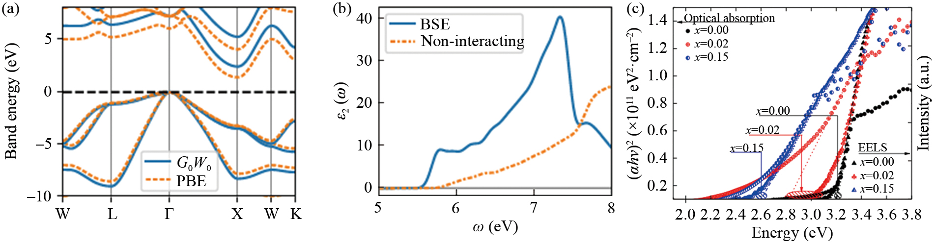
As shown in Figs. 1(a) and 1(b), the band gap of 3C-SiC was calculated by Perdew-Burke-Ernzerhof (PBE) functional,
and the result obtained was 1.4 eV. Still, after considering the GW approximation, the band gap calculated by the G0W0 method was 2.3 eV, which is very close to the experimental value of 2.36 eV [29]. In the discussion of the band gap of (ZnO)1–x(GaN)x alloy by Olsen et al., a GW approximation was used to calculate the band gap of the system, and the results are
shown in Fig. 1(c), which are in good agreement with the experimental values [32]. The GW approximation is a many-body perturbation theory based on the one-body Green's function,
which provides a more rigorous framework for describing electronic structure than
conventional methods [33–37]. At its core is the exchange-correlation self-energy function, which is analogous
to the exchange-correlation potential in the Kohn-Sham density functional theory.
Unlike the exchange-correlation potential, the exchange-correlation self-energy is
a spatially nonlocal, energy-dependent, non-Emilian function that includes all non-classical
electronic interaction effects beyond the Hartree approximation. The photoelectron
spectrum (PES) and inverse photoelectron spectrum (IPS) associated with the quasiparticle
excitation energy spectrum can be obtained directly from the self-energy function,
and these energy spectra can be measured experimentally. The exact self-energy function
follows a set of self-consistently coupled integral differential equations known as
the Hedin equation [36, 38]. However, since the solution of this equation is extremely difficult to find in
complex systems, approximations must be introduced in practical applications. The
most commonly used approximation is the GW approximation, in which the self-energy function in the time-space domain is expressed
as the product of the one-body Green's function G and the shielding Coulomb action W. The GW approximation is used to solve the Hedin equation. Although the GW approximation provides an effective computational framework, the numerical solution
of the Hedin equation still faces the challenges of complex program implementation
and high computational complexity. In practical studies, a commonly used approximation
is the G0W0 method, in which G and W are calculated based on the single-electron orbital energy and wave function, respectively,
at some mean-field approximation (H0) [39].
The GW approximation method enhances the DFT, thereby improving the accuracy with which
it characterizes the dynamic effects of electrons and significantly improving the
accuracy of bandgap prediction [41, 42]. Recent studies have demonstrated that the GW method has become a standard and effective tool for bandgap prediction in wide bandgap
materials. Rinke et al. applied the GW approximation to correct the bandgap of GaN, finding that it more accurately matched
experimental results compared to DFT, which underestimated the bandgap [41]. Notably, temperature effects also play a critical role in bandgap modulation. As
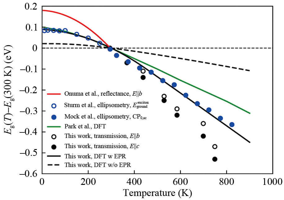
demonstrated by Lee et al., the electronic structure of β-Ga2O3 exhibits significant temperature dependence due to electron-phonon interactions and
thermal expansion [42]. Their combined first-principles and experimental study revealed a bandgap reduction
of over 0.5 eV between 0 and 900 K (Fig. 2), with electron-phonon renormalization identified as the dominant mechanism. This
work highlights the necessity of incorporating temperature effects alongside advanced
exchange-correlation corrections for accurate bandgap predictions in device-operating
conditions. The study achieved a more accurate energy band structure by combining
the GW method with DFT, providing a theoretical basis for optimizing GaN's performance in
high-power applications.
In addition to the traditional DFT and GW methods, hybrid functional approaches have been widely adopted in recent years for
studying wide bandgap semiconductors. By incorporating nonlocal exchange-correlation
functions, these methods effectively enhance the accuracy of bandgap calculations,
addressing the limitations of DFT [43].
Back in the 1990s, Becke, together with Bylander and Kleinman, almost simultaneously
proposed the introduction of a nonlocal exchange-correlation potential to make corrections
to the electronic structure of the system [43, 44]. This approach is no longer limited to the Kohn-Sham theoretical framework. Seidl
et al. later systematized this approach [45]. They changed the definition of the single reference. This redefinition ensured
the approach was strictly unified within the DFT framework. It led to the development
of generalized Kohn-Sham (GKS) theory. These methods perform well in specific cases.
However, they still fail significantly in calculations of total energy and other properties.
In recent years, high-throughput computing and machine learning methods have gradually
become popular directions in wide bandgap semiconductor research. And artificial intelligence
based on big language models is also shining in the industrial sector [46]. By combining high-throughput computing and machine learning, researchers can more
efficiently screen materials with excellent properties [47–54]. A methodology paradigm that has demonstrated cross-domain effectiveness in fields
ranging from wearable sensor optimization to robotic motion control systems [55, 56]. For example, Chen et al. utilized pymatgen and matminer to extract data from the
materials project, encompassing 3720 ABX3-type compounds and 2660 A2B(I)B(II)X6-type compounds. This effort enabled the identification of key material characteristics
with accurately predicted band gaps and formation energies. To estimate missing data,
the random forest algorithm was employed, followed by using tolerance and octahedral
factors to screen for stable chalcogenide structures, thereby improving data quality.
A subsequent SHAP (SHapley Additive exPlanation) analysis was performed to determine
the most influential descriptors. The results indicate that higher formation energies,
a large number of transition metals, and a considerable presence of d-orbital valence
electrons are critical for forming narrow bandgap perovskites. In contrast, a higher
number of f-orbital electrons and large electronegativity differences between elements contribute
to the formation of wide bandgap perovskites. Additionally, Shen et al. developed
a hierarchical material screening framework (HMSF) to identify ultra-wide bandgap
materials. The framework is similar to graph-based path-planning strategies in robotic
systems [57]. They established a correlation between material chemistry and properties and adjusted
hyperparameters in the machine-learning algorithm to enhance prediction accuracy via
Bayesian optimization. This approach led to the discovery of four previously unknown
ultra-wide bandgap materials characterized by suitable forbidden bandwidths, exceptional
thermal stability, a pronounced deep ultraviolet optical response, and low electronic
effective masses. These achievement highlights the significant potential of machine
learning in accelerating material design.
In the study of semiconductor materials, it has been found that introducing defects
and doping, among other things, has a significant effect on the electronic structure
of semiconductors. For example, co-doping and Co-Al Co-doping in ZnO were discussed
by Khan et al. It was found that after Co doping, the material exhibited antiferromagnetism,
while after Co Al co-doping, there was a transformation of the antiferromagnetic phase
into a ferromagnetic phase, and the energy of the antiferromagnetic state was higher
than that of the ferromagnetic phase by 184 meV, which is much higher than the thermal
motion energy at room temperature [58]. With this energy difference, the Curie temperature of the system was calculated
by mean-field theory to be 690 K. Meanwhile, the optical absorption spectrum shows,
with the increase of Co concentration, the band gap of ZnO and the position of the
d-d transition peak of Co ions show blueshifts and redshifts behaviors, respectively;
with the Co concentration increases, the intensity and width of the d-d transition
peaks decrease. In addition, Co Al co-doping not only increases the band gap but also
generates new absorption peaks in the infrared and visible regions. This work demonstrates
the modulation of ZnO optoelectronic and magnetic properties by Co doping and Co Al
co-doping. It provides theoretical support for applying ZnO-based materials in future
electronic and optoelectronic devices. Beyond chemical modifications, environmental
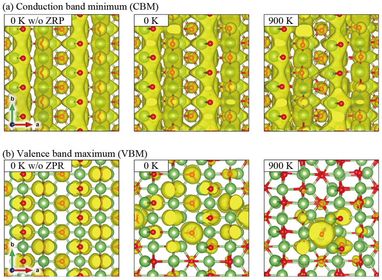
factors such as temperature also profoundly reshape electronic properties. Lee et
al. demonstrated that thermal lattice vibrations in β-Ga2O3 induce band edge localization, particularly for the valence band maximum (VBM), as
shown in their charge density isosurfaces (Fig. 3) [42]. This localization leads to increased hole effective masses at elevated temperatures,
directly impacting carrier mobility and device performance. Such findings emphasize
the interplay between intrinsic defects, extrinsic dopants, and thermodynamic conditions
in determining semiconductor behavior.
First-principles calculations have played a crucial role in the study of the electronic
structure of wide bandgap semiconductors, and significant progress has been made in
the prediction and optimization of the bandgap. By using advanced computational methods
such as DFT, GW approximation, and hybrid functional methods, researchers can gain a deeper understanding
of the electronic properties of wide bandgap semiconductors. In addition, emerging
research methods such as high-throughput computing, machine learning, and defect engineering
offer more opportunities for material design and performance optimization. With continued
improvements in computational accuracy and the emergence of new methods, researchers
are able to more precisely control the electronic properties of wide bandgap semiconductors,
providing a solid theoretical foundation for their applications in fields such as
high-power electronics, optoelectronics, and quantum computing.
2.2 Calculation of optical properties
Optical properties are one of the important characteristics of wide bandgap semiconductors,
as they directly determine the potential applications of these materials in optoelectronic
devices, including photodetectors, lasers, solar cells, and light-emitting diodes
[59–61]. Through first-principles calculations, researchers can analyze the optical response
of materials in detail, including absorption spectra, reflectance, and optical bandgap.
This, in turn, provides theoretical support for the optimization of the materials'
optoelectronic properties. The optical properties of wide bandgap semiconductors are
closely related to their electronic structures; therefore, accurate prediction of
optical properties is crucial for the design and application of the materials [62–64].
The accurate calculation of the optical properties of materials by DFT, especially
the calculation and prediction of absorption spectra and optical bandgap, has gradually
become a research hotspot. The GW-BSE method has an important position in this field and has become one of the standard
methods for predicting optical properties. The GW-BSE method is a computational approach grounded in many-body perturbation theory,
which is employed to investigate the quasiparticle and optical characteristics of
materials [65–67]. It combines the GW approximation and the Bethe-Salpeter equation (BSE) to accurately calculate the bandgap
and exciton properties of materials from first principles. The GW approximation, as previously mentioned, is a method used to calculate the quasiparticle
properties of materials by approximating the electron self-energy to the quasiparticle
energy and wave function. It is able to provide more accurate band gap values than
conventional DFT. The BSE is mainly used to study the optical properties of materials,
especially exciton effects. It has been demonstrated to be a highly effective tool
for predicting the optical response of materials by considering the electron-hole
interaction [68–70]. The BSE approach treats the electron-hole pair as a whole, known as an exciton,
and calculates the energy and wave function of its excited state. The GW-BSE method integrates the GW approximation and BSE, enabling the simultaneous consideration of quasiparticle and
exciton effects. It is widely regarded as one of the most precise methodologies for
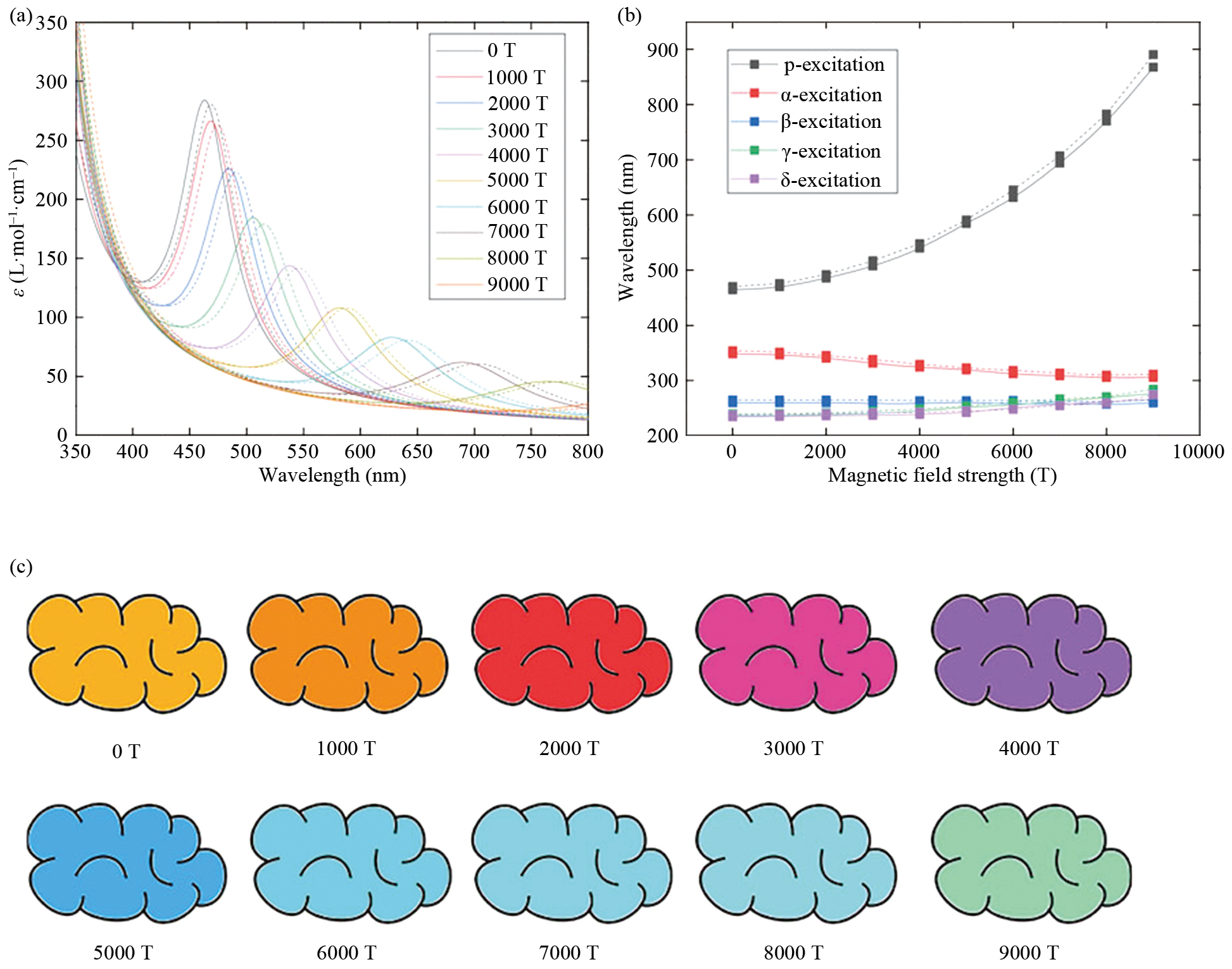
calculating quasiparticle and optical properties of condensed matter systems [65, 67, 71, 72]. Holzer et al. investigated how GW-BSE can be used to calculate molecular excitation energies in strong magnetic fields.
They extend the application of these methods by introducing the Bethe-Salpeter equation
with the GW approximation into calculations in strong magnetic fields. They also provide a new
computational framework that can accurately describe molecular excitation energies
and optical properties in the presence of strong magnetic fields [71]. In addition, the work is compared with reference data on the excited energies of
the triplet states of 36 small to medium-sized molecules. The results verify the validity
of the method under strong magnetic fields, demonstrating the significant effect of
strong magnetic fields on the optical properties of molecules. Excitation energy calculations
for different molecules under strong magnetic field conditions yielded significant
changes in the optical properties. As demonstrated in Fig. 4, the color of tetracene undergoes a transition from orange to green as the magnetic
field strength increases from 0 to 9000 T. This color change can be accurately predicted
by the GW-BSE method. The calculation of the excitation energy of a strong magnetic field based
on the GW-BSE method proposed by Holzer et al. establishes a novel theoretical framework for
the study of the optical properties of molecules in extreme environments. This work
not only expands the application of the GW-BSE method but also provides a powerful tool for the accurate characterization of
the optical properties of molecules under strong magnetic fields. Future studies can
build on this foundation to further explore the excitation energy spectra and optical
behaviors of different types of molecules, especially complex molecular systems, in
high-intensity magnetic fields. With the continuous development of computational methods,
combined with more efficient many-body theories and modern computational techniques,
it is expected to be able to deal with larger and more complex molecular systems and
to reveal the far-reaching effects of magnetic fields on the excitation energies of
molecules.
The GW-BSE method has been successful in calculating the optical properties of materials.
However, we should also pay attention to the selective modulation of optical properties
by heterojunctions and strains, and so on [73–77]. Feng et al. found that the strain of the material can have an important effect
on the optical properties. For example, Feng et al. studied the electronic and optical
properties of van der Waals heterostructures stacked with g-ZnO and Janus-WSSe monolayers
using VASP to calculate their properties [78]. They used the hybridized, generalized Heyd-Scuseria-Ernzerhof (HSE) method to obtain
more accurate band gap values. The electronic structure and band alignment of AB-stacked
g-ZnO/Janus-WSSe heterostructures are discussed in the work. It is found that the
configuration has a typical type II band alignment, i.e., the conduction band minimum
(CBM) and the valence band maximum (VBM) are in different materials. This band alignment
facilitates the separation of photogenerated electrons and holes, thus improving the
photocatalytic efficiency. In addition, due to the difference in the figure of merit
between g-ZnO and Janus-WSSe (ΔΦ = 0.533 eV), electrons are transferred from the g-ZnO layer to the Janus-WSSe layer,
forming an intrinsic built-in electric field. This built-in electric field promotes
the separation of photogenerated electron-hole pairs, which enhances the photocatalytic
efficiency. A similar enhancement mechanism was observed in the S-type heterojunction
of amorphous/crystalline carbon nitride, where the optimized interfacial charge transfer
led to a significant improvement in the reduction efficiency of CO2 [79]. Interestingly, the optical absorption coefficients of the AA-stacked and AB-stacked
heterostructures show unique characteristics under different strains. Negative stretching
increases the ultraviolet (UV) absorption and decreases the visible absorption, while
positive stretching decreases the UV absorption and increases the visible absorption.
Furthermore, the AB-stacked g-ZnO/Janus-WSSe heterostructure exhibits excellent photocatalytic
water decomposition. The photoexcited electrons were transferred to the conduction
band of the Janus-WSSe layer, while the photoexcited holes were transferred to the
valence band of the g-ZnO layer. In the Janus WSSe layer, the collected photoexcited
holes can drive the generation of oxygen; in the g-ZnO layer, the collected photoexcited
electrons can drive the generation of hydrogen.
van der Waals heterostructures can be formed by stacking different two-dimensional
materials. The combination of two or more materials into a heterojunction can effectively
modulate the electronic and optical properties of the material [80–83]. While heterostructure engineering focuses on interfacial effects, chemical doping
provides an alternative pathway for optical tuning. He et al. systematically compared
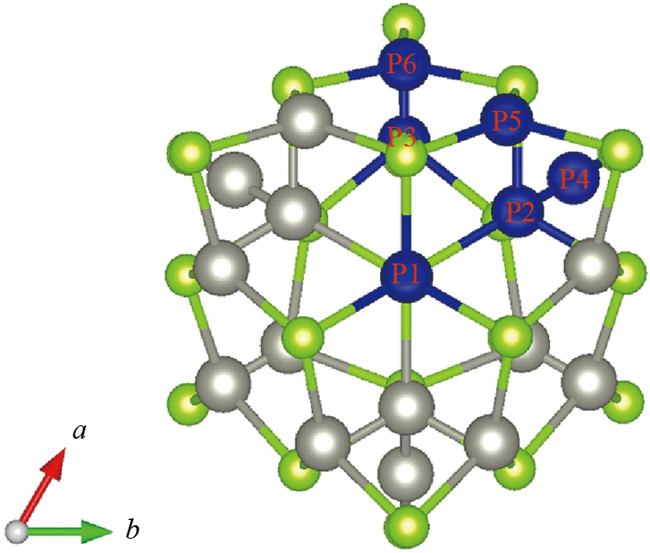
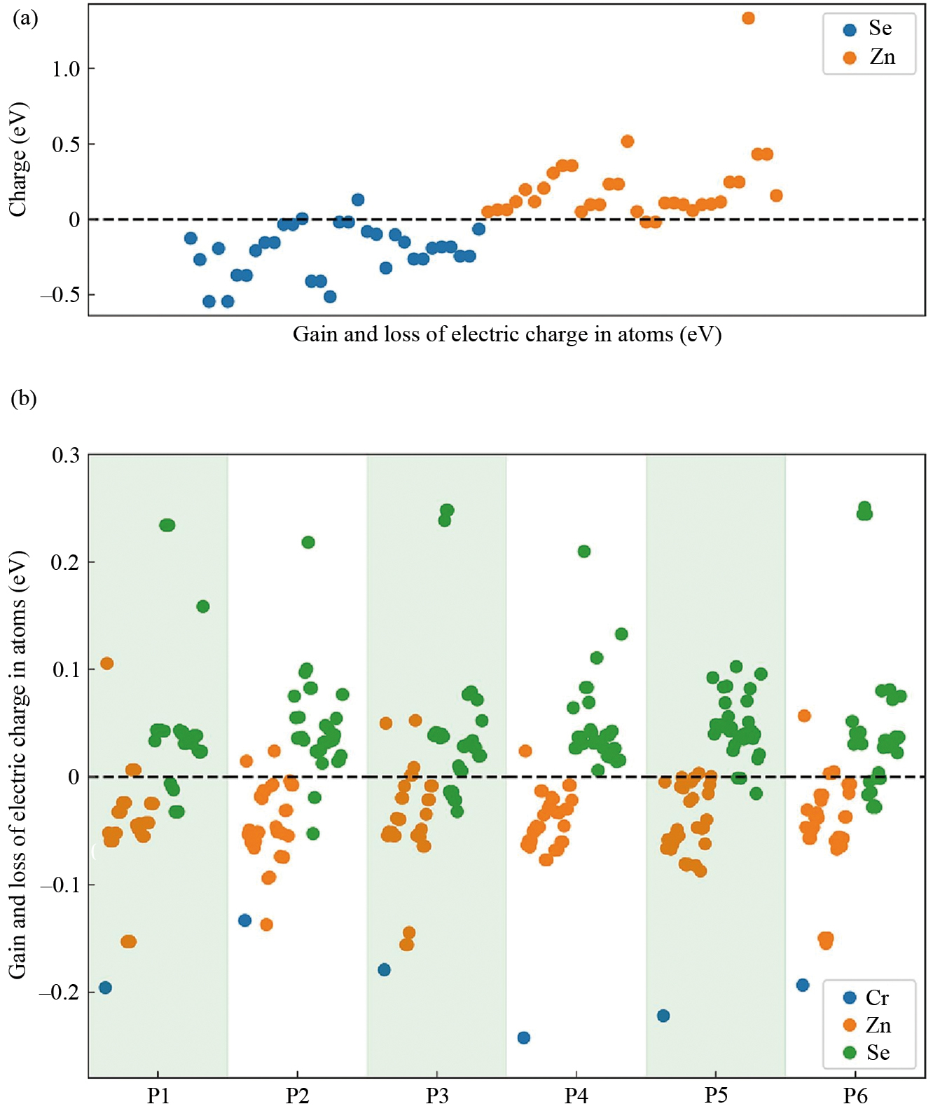
Cr doping positions (center, radius ½, surface) in ZnSe nanowires (NWs) (Fig. 5), revealing that mid-gap defect states from Cr(d)-Se(p) hybridization dominate absorption
characteristics [84]. Their Bader charge analysis (Fig. 6) further shows localized charge redistribution around dopants, creating defect-induced
absorption peaks distinct from heterojunction-mediated modifications. This approach
often achieves a better result and is a hot research topic in the academic community.
In 2023, Mustafa et al. investigated the electronic and optical properties of photodetectors
based on multilayer graphene/MoS2 heterostructures [85]. Their work systematically investigated the electronic and optical properties of
multilayer graphene/MoS2 heterostructures. The results show that the band gap of MoS2 can be significantly tuned by introducing graphene layers, which can be reduced by
up to 36.3 meV, making the heterostructures promising for applications in photodetectors.
Meanwhile, the optical absorption coefficients of the graphene/MoS2-based heterostructures are significantly enhanced in the visible to ultraviolet region,
especially at 1551 nm (0.8 eV) and 1240 nm (1 eV), indicating an enhanced light absorption
capability in these wavelength ranges. In addition, these heterostructures exhibit
nonlinear optical behavior from the infrared to the visible region, which has important
implications for photonic devices, especially photodetectors.
From the above, we can realize that optical property calculations are the key to understanding
and optimizing the optoelectronic performance of wide bandgap semiconductors. With
the advancement of computational methods, especially the application of GW-BSE method, researchers are able to predict the optical response of wide bandgap
semiconductors more accurately. In addition, the influence of factors such as heterojunction,
stress modulation, and surface interfacial effects on the optical properties has become
a hot topic of current research. Through these studies, more accurate theoretical
support and design guidance can be provided for the application of wide-bandgap semiconductors
in optoelectronic devices.
2.3 Calculation of thermal properties
As one of the core research areas in condensed matter physics and materials science,
the thermal properties of materials are directly related to key engineering and technological
issues such as energy conversion efficiency, reliability of electronic devices, and
thermal protection systems in aerospace. Traditional experimental methods for measuring
thermal conductivity, thermal expansion coefficient, and lattice vibrational properties
face many challenges: the difficulty of in-situ characterization under extreme conditions (high temperature/high pressure), the bottleneck
of accurate quantification of the interfacial thermal resistance of low-dimensional
materials, and the limitations in analyzing the heat transport mechanism of new complex
compounds. In this context, first-principle computational methods, with their unique
advantages based on the fundamental principles of quantum mechanics, have gradually
emerged as an important research paradigm for revealing the microscopic mechanisms
of the thermal properties of materials. It is well known that thermal properties are
key indicators of the stability and application performance of wide bandgap semiconductors
in high-temperature environments [86–88]. Recent experimental breakthroughs in the thermal management of AlN further validate
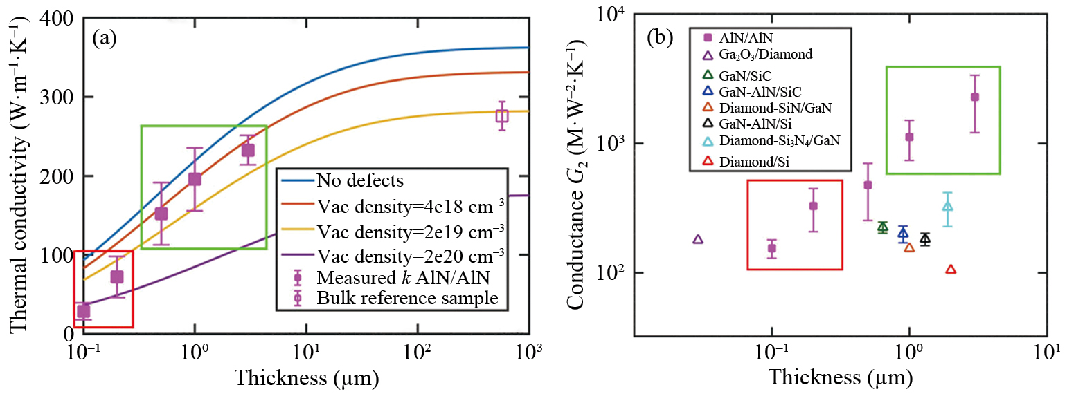
this thesis. Alvarez-Escalante et al. demonstrated that homoepitaxial AlN thin films
achieve exceptional thermal conductivity up to 195.71 W·m–1·K–1 at 1 μm thickness (Fig. 7(a)), approaching 57% of the bulk theoretical value (340 W·m–1·K–1) [89]. Remarkably, their frequency domain thermoreflectance (FDTR) measurements revealed
ultrahigh thermal boundary conductance (G) exceeding 2590 MW·m–2·K–1) for 3 μm films (Fig. 7(b)), attributed to atomic-level interface control via Al-assisted surface cleaning.
This represents a 10-fold improvement over heteroepitaxial systems like GaN/SiC (G≈230 MW·m–2·K–1), effectively overcoming the interfacial resistance bottleneck in traditional low-dimensional
materials. With the increasing application of semiconductor materials in high-power
electronic devices, optoelectronic devices, and thermoelectric devices, it becomes
particularly important to accurately calculate and optimize the thermal properties
of materials, such as thermal conductivity, specific heat capacity, and thermal expansion
[90–93]. Thermal properties are directly related to the thermal stability, thermal diffusivity,
and energy conversion efficiency of materials at high temperatures [94, 95]. Therefore, first-principles calculations provide a powerful theoretical tool to
study these properties and are especially indispensable in the design and performance
optimization of wide bandgap semiconductor materials.
In 1996, Mahan and Sofo presented a study on maximizing the eutectic value of thermoelectric
materials by optimizing the electronic structure [96]. They unified the electrical conductivity, thermal potential, and thermal conductivity
as integrals of a transport distribution function and derived a mathematical function
of the transport distribution that maximizes the optimum value. Specifically, they
used the Boltzmann equation to describe the transport coefficients and introduced
a transport distribution function related to the velocity, lifetime, and dispersion
relations of the electron population. By using a transport distribution in the form
of a delta function, the thermoelectric optimum can be maximized. This suggests that
the electron energy distribution involved in the transport process should be as narrow
as possible to achieve higher thermoelectric efficiency. This study provides a new
theoretical perspective for the design of high-efficiency thermoelectric materials,
which is of great significance for the subsequent improvement of the optimum value
of thermoelectric materials.
In addition, DFT calculations show significant potential in the study of the thermal
properties of two dimensional (2D) materials. Tang et al. found that nanohoneycomb-pleated
PbTe monolayers have very low lattice thermal conductivity (0.75–0.79 W·m–1·K–1 at 900 K) and high electron mobility (499.552 cm2·V–1·s–1) through an in-depth study of PbTe [97]. They calculated the phonon dispersion relation using density functional perturbation
theory (DFPT), confirmed the kinetic stability of the system, and quantified the phonon
scattering effect. The folded structure induces strong phonon anharmonicity, which
reduces the lattice thermal conductivity at 900 K to 0.75–0.79 W·m–1·K–1, which is two orders of magnitude lower than that of conventional bulk materials.
Combined with Boltzmann transport theory calculations, the system exhibits a Seebeck
coefficient of 1.574 mV·K–1 and a thermoelectric figure of merit (ZT) of 1.55 in the 300–900 K range. The performance
enhancement is mainly attributed to the optimization of carrier transport under electron-phonon
coupling. This study has successfully established a theoretical correlation model
from the atomic-scale electronic structure to the mesoscale thermal transport properties,
which provides a quantitative research framework for the rational design of low-dimensional
thermoelectric materials. Further, recent advances in structural design further demonstrate
the versatility of 2D materials in thermal-electronic coupling. Zhao et al. systematically
investigated strain-modulated anomalous thermal transport in porous buckled X-AlN
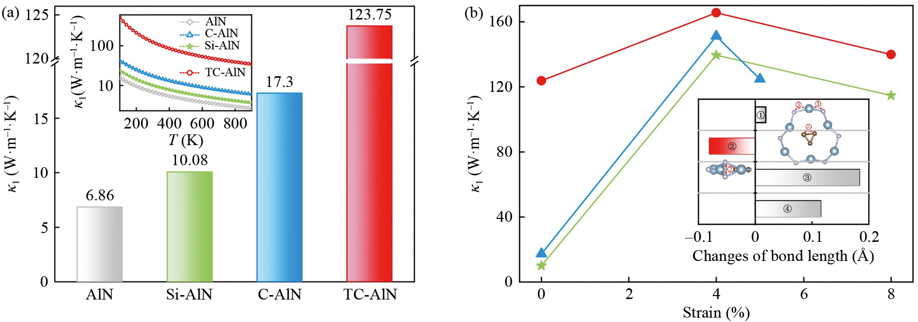
(X=C, Si, TC) monolayers through evolutionary structural search and first-principles
calculations [98]. As shown in Fig. 8(a) of their work, the lattice thermal conductivity of TC-AlN reached 123.75 W·m–1·K–1 at 300 K, 17 times higher than pristine AlN, due to strong covalent bonds suppressing
out-of-plane phonon scattering. Remarkably, their Fig. 8(b) revealed a non-monotonic thermal conductivity response under biaxial strain: an initial
increase peaking at 4% strain (165 W·m–1·K–1) followed by decline, arising from competition between enhanced N-N bond strength
reducing anharmonicity and phonon mode softening at higher strains. This strain-engineered
thermal switching mechanism provides new insights for dynamically controlling heat
dissipation in semiconductor devices. Notably, reducing the dimensionality of the
material to two dimensions has also been shown to be an effective way to improve the
thermodynamic stability. Li et al. predicted two BeH2 monolayer structures (α-BeH2 and β-BeH2) by performing a global search via a particle swarm optimization method and found
that these two structures have high thermodynamic stability and mechanical strength
[99]. The study also unexpectedly found that α-BeH2 has a negative Poisson's ratio, which is rare in 2D materials. Since the beryllium
hydride monolayer has the same number of electrons as graphene, its 2D structure is
highly feasible in experiments, which provides a strong theoretical basis for the
experimental preparation of monolayer BeH2. The above studies have successfully revealed the microscopic mechanism of the material
properties at the theoretical level, providing a new perspective for further understanding
the physical connotation of the materials.
The thermal properties of materials are a key area of research in condensed matter
physics and materials science, directly affecting the efficiency of energy conversion
and a wide range of engineering applications. In polymer nanocomposites, morphologically
tailored nanostructures have been shown to achieve exceptional breakdown field strength
(>10 MV·cm–1) alongside giant electrocaloric effects, illustrating the universal value of microstructure
design in thermal-electrical property optimization [100]. Traditional experimental methods have significant limitations in in-situ characterization under extreme conditions of high temperature and pressure, in quantifying
thermal resistance at low-dimensional material interfaces, and in resolving heat transport
mechanisms in complex materials. First-principles calculation, with its essential
advantages based on quantum mechanics, provides a powerful tool for revealing the
microscopic mechanisms of the thermal properties of materials. It is particularly
important for the systematic understanding of thermal properties such as thermal conductivity,
specific heat capacity, and thermal expansion of materials. Through first-principles
calculations, the thermal behavior of materials in complex environments can be accurately
predicted, and on this basis, materials design and performance optimization can be
carried out, providing theoretical basis and guidance for the research and development
of high-efficiency thermoelectric materials, wide-bandgap semiconductors, and novel
low-dimensional materials, and promoting the continuous development of the frontiers
of materials science.
2.4 Doping and defect engineering
Doping and defect engineering is a fundamental strategy for optimizing the performance
of wide bandgap semiconductors. This approach is achieved through precise control
of energy band structures, effective modulation of carrier concentrations, and strategic
management of surface states, etc., which collectively enhance material functionality
[101–105]. By implementing elemental doping strategies (e.g., rare earth ion implantation
or transition metal substitution) as well as controllable defect construction (including
vacancy defects and dislocation modulation, etc.), researchers are able to achieve
precise modulation of material properties [106–109]. Taking GaN-based compounds and wide bandgap oxide systems in third-generation semiconductor
materials as an example, advanced defect engineering design not only significantly
improves carrier mobility (1000–1500 cm2·V–1·s–1) and breakdown field strength (>3 MV·cm–1), but also realizes linear enhancement of photoelectric response in the visible-ultraviolet
region (about 40% increase in external quantum efficiency (EQE)) through defect energy
level modulation [110–112]. Recent advances in defect stabilization mechanisms further expand the scope of
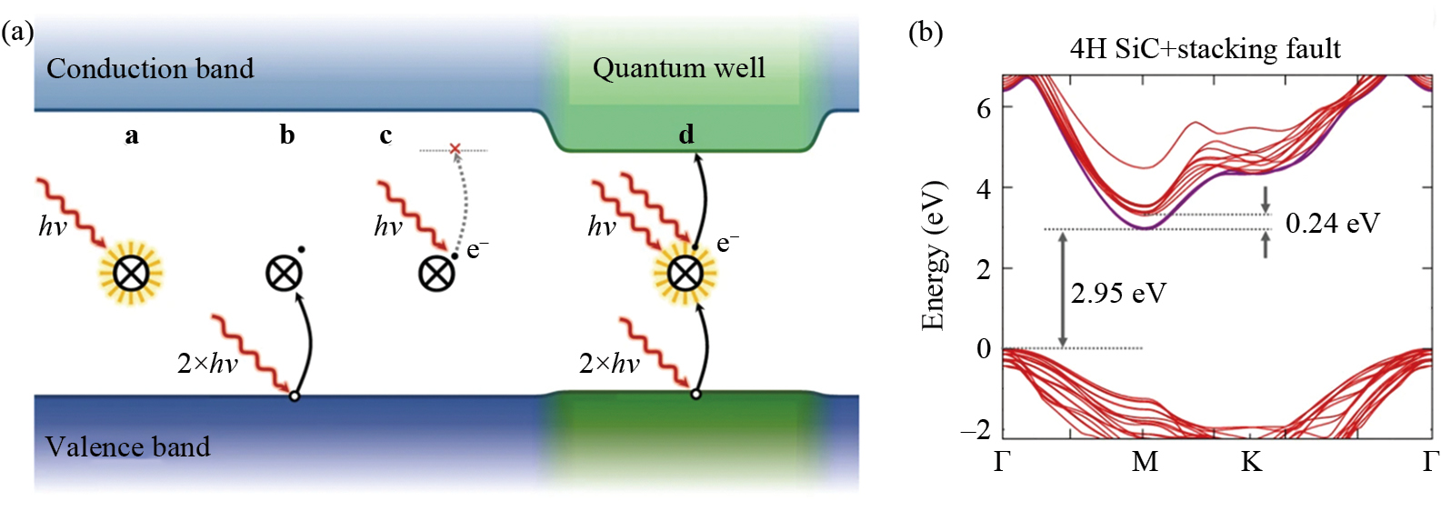
defect engineering. Ivády et al. demonstrated that quantum wells formed by Frank-type
stacking faults in 4H-SiC can stabilize divacancy spin qubits by locally lowering
the conduction band minimum (~0.24 eV reduction) through polytypic 6H-SiC inclusions
(Fig. 9). This quantum confinement effect enables selective ionization of divacancy dark
states (VV⁻) under optical excitation, significantly enhancing charge state stability
during room-temperature spin manipulation [113]. Such crystallographically engineered environments provide a materials-centric solution
to persistent challenges in photoionization-induced charge fluctuations. In addition,
recent advances in 2D van der Waals semiconductors, such as CrSCl with intrinsic p-type
conductivity and multipolarity coexistence, further demonstrate the potential of defect
engineering beyond conventional doping paradigms [114]. This micro-regulation technology has been successfully applied to high-power electronic
devices, deep-ultraviolet LEDs, photovoltaic catalysis and other cutting-edge fields,
and the industrialization conversion rate of relevant research results has been increased
by nearly 70% compared with the traditional process, promoting the continuous development
of wide bandgap semiconductor materials toward high integration and low energy consumption.
Along this technological path, diamond, as a typical wide-band semiconductor material,
shows significant advantages in the field of miniaturization of high-power electronic
devices by virtue of its ultra-high breakdown field strength (>10 MV·cm–1) and excellent carrier mobility (≥2000 cm2·V–1·s–1) [115]. Although significant progress has been made in boron-doped p-type diamond (BDD),
efficient n-type doping is still a key technological bottleneck limiting the development
of diamond devices due to the high dissociation energy property of the donor impurity.
To address this challenge, Liu's research team successfully prepared boron-rich layers
of 1–1.5 μm thickness on the (111) crystal surface of boron-doped diamond single crystals
using the temperature gradient growth (TGG) method [116]. This study shows that by precisely tuning the experimental parameters during diamond
crystallization, the controllable formation of B-O complexes can be achieved, which
in turn induces the material to exhibit n-type conducting properties. Mechanistic
analysis based on first-principles calculations indicates that the B3O and B4O complexes form shallow donor energy levels in the diamond lattice, which is essentially
responsible for the n-type semiconductor behavior. It is particularly noteworthy that
the formation energies of these two complexes are as low as – 4.27 eV and – 6.05 eV,
respectively, indicating their significant thermodynamic formation advantage in the
diamond system. Further comparative analysis confirms that the B4O complexes have the lowest formation energies compared to other defect configurations,
thus dominating the crystal growth process. This study successfully breaks the technical
bottleneck of n-type diamond preparation by innovatively introducing the doping strategy
of B-O complexes, which provides a new research direction for the development of diamond-based
semiconductor devices. This work not only elucidates the electronic structure regulation
mechanism of the compound defects but also lays an important theoretical foundation
for the subsequent performance optimization of diamond electronic devices.
Besides diamond, cubic boron nitride (c-BN) is another semiconductor material with
great application potential. They serve as promising ultra-wideband semiconductors
in the field of high-power, high-frequency electronics, and experimental measurements
of their carrier mobility have long differed significantly. To elucidate the intrinsic
physical mechanisms, Sanders's team systematically revealed the microscopic properties
of carrier transport in these two types of materials and their governing laws for
device performance through a first-principles approach [117]. In the study, density functional theory combined with many-body perturbation theory
(G0W0 quasiparticle correction) was used to accurately calculate. It obtains the bandgap
values of 5.66 eV and 6.80 eV for diamond and c-BN, respectively. It is found that
the phonon-limited electron mobility at room temperature is similar for both materials
(diamond: 1790 cm2·V–1·s–1, c-BN: 1610 cm2·V–1·s–1) by density functional perturbation theory using the maximally localized Wannier
function method, but the hole mobility of c-BN (80.4 cm2·V–1·s–1) shows a two order of magnitude difference compared to that of diamond (1970 cm2·V–1·s–1). The phenomenon is attributed to the strong inelastic scattering effect induced
by the significant increase in the effective mass of holes at the top of the c-BN
valence band. The study also reveals the dynamic evolution properties of the carrier
scattering mechanism: lattice scattering dominates in the low temperature region,
while neutral impurity scattering becomes the main constraint at high doping concentrations.
The theoretical model predicts the n-type c-BN and p-type diamond mobility with an
error of less than 20%, verifying the reliability of the computational framework.
This work not only elucidates the competition mechanism between intrinsic scattering
and defect scattering in ultra-wide bandwidth semiconductors but also points out that
the inherent hole mobility defect of c-BN will seriously limit its application prospects
in bipolar devices, providing theoretical guidance for material performance optimization.
The above systematically discusses the intrinsic properties of two types of typical
wide-band semiconductor materials and reveals the regulatory mechanisms of doping
and defect engineering on their energy band structures and carrier transport properties.
In-depth analysis reveals that the key scientific issues that constrain the performance
enhancement of these semiconductor devices focus on the precise analysis of defect
behavior and the effective suppression of their harmful effects. Using hybridization
density functional theory calculations, Gao et al. systematically investigated the
local structural relaxation properties, formation energy evolution laws, and their
electron migration properties of neutral/charged intrinsic point defects (including
vacancy, interstitial, and antisite defects) in GaN, AlN, and InN crystal systems
[118]. By comparing the jump energy levels associated with the Fermi energy levels, it
is found that Ga interstitial, nitrogen vacancy, N interstitial, In antisite, and
In interstitial in the GaN system are stable only in the positive charge state with
a donor energy level. While In vacancy are more stable in the neutral state, the other
defects show both donor and acceptor behavior. Theoretical analysis of defect states
shows that nitrogen vacancy in p-type nitrides and gallium/aluminum vacancy in n-type
nitrides are the most stable defect configurations, a finding that provides a microscopic
explanation for self-compensating effects in nitride materials and elucidates the
physical cause of defect-induced n/p-type doping efficiency decay. It is also confirmed
that the diffusion rate of nitrogen interstitials is significantly higher than that
of vacancy defects, which directly leads to the low concentration characteristic of
nitrogen interstitials and nitrogen-based defect complexes in nitrides. It is particularly
noteworthy that the trends of formation energies, jump energy levels, and migration
barriers of nitrides show significant correlations with their intrinsic atomic sizes
and the width of the bandgap. The theoretical framework for defect identification
and control established in this work is of great importance in guiding the performance
optimization and reliability enhancement of nitride semiconductor devices.
Doping and defect engineering play a critical role in the performance modulation of
broadband semiconductor materials, the core of which lies in the precise modulation
of energy band structure, carrier dynamics and defect behavior through atomic-scale
design. Using diamond and cubic boron nitride (c-BN) as examples, the study reveals
the intrinsic constraints on carrier mobility in ultrawide-bandgap semiconductors:
Although diamond has excellent carrier transport properties, its n-type doping has
long been limited by the high dissociation energy of the sizing impurity, and innovative
doping strategies based on the B-O complexes provide a new way to break the bottleneck
by constructing a shallow sizing energy level; while in c-BN, the significant increase
in the effective mass of the hole leads to a significant increase in the effective
mass of the hole. The significant increase in effective mass leads to a sharp decrease
in hole mobility, highlighting the inherent defects of its bipolar device applications.
In nitride semiconductors, the defect-induced self-compensation effect and the dynamic
evolution characteristics further reveal the microscopic roots of the doping efficiency
decay. Complementary studies on GaN systems highlight the tunability of defect-mediated
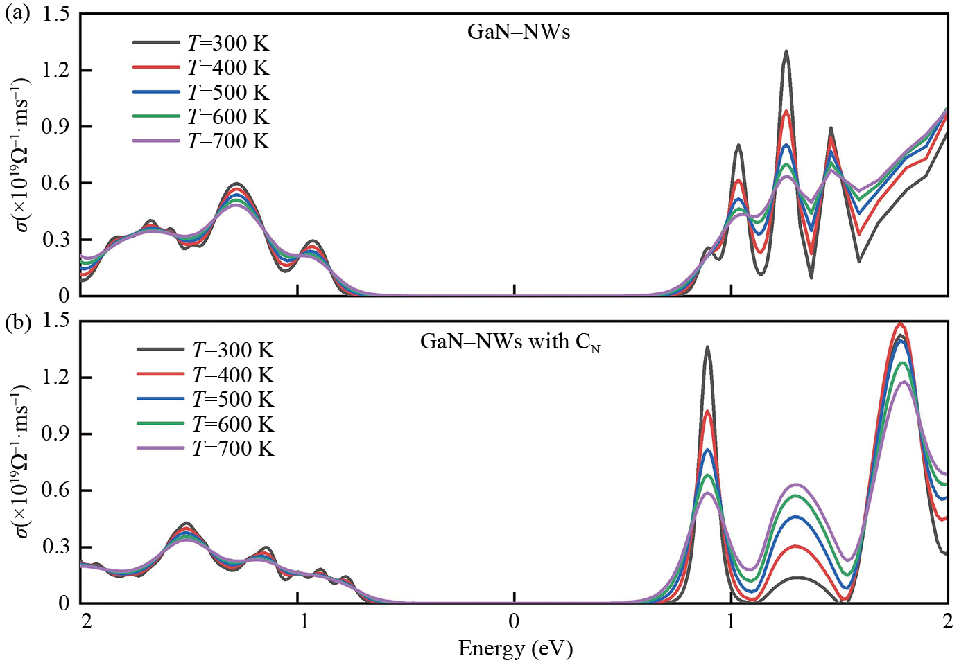
properties. Liao et al. systematically investigated CN point defects in GaN NWs, revealing their dual role in enhancing electrical conductivity
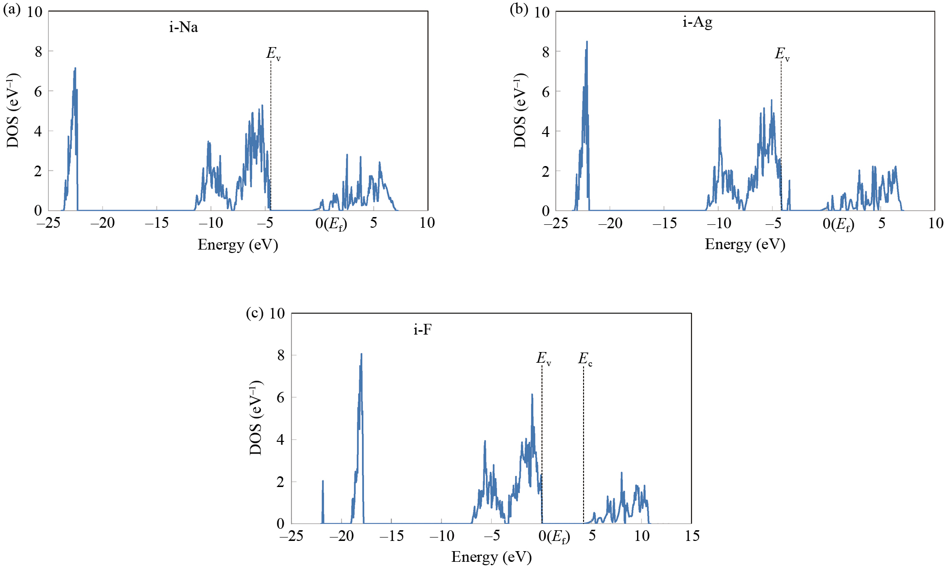
(1.15×10¹⁴ W·m–1·K–1 at 700 K) while suppressing Seebeck coefficients (0.0008 V·K⁻¹ at 700 K). As shown
in Figs. 10(a) and 10(b), the increased density of states near the Fermi level from C(p)-N(p) orbital hybridization
drives these effects, offering a trade-off strategy for optimizing thermoelectric
performance [119]. Theoretical calculations based on the ab initio methods have deeply resolved the
correlation mechanism between defect formation energy and electronic structure, providing
an important theoretical basis for suppressing harmful defects and optimizing doping
paths. Taken together, these studies show that the synergistic design of atomic-level
defect engineering and energy-band engineering, which reconciles the contradiction
between intrinsic material properties and doping regulation, is the key way to advance
wide bandgap semiconductors toward high-performance and high-reliability devices.
3 Application of first-principles calculations to the design of wide bandgap semiconductor
devices
As materials science enters the era of "atomic engineering", the quantum correlation
between microscopic electronic structures and their macroscopic properties has become
the key to overcoming technical bottlenecks. The traditional experience-driven materials
research and development model is limited by high costs and a long trial-and-error
cycle, making it difficult to meet the urgent demand for high-performance materials
in strategic fields such as clean energy and quantum information. In this context,
first-principles calculations, which are based on the fundamental laws of quantum
mechanics and require no empirical parameters, are reshaping the theoretical framework
and practical ways of materials design. By solving the many-body Schrödinger equation,
the method can accurately analyze the intrinsic physical properties of materials (e.g.,
energy band topology, defect dynamics, interfacial charge transport, etc.) and provide
atomic-scale insights into key issues such as predicting cell electrode mobility barriers,
chalcogenide defect suppression, and Schottky junctions [120–122]. With the innovation of density functional theory algorithms and the leap of supercomputing
technology, its application boundary has been expanded from static physical property
calculations to dynamic multiscale modeling, and through deep fusion with molecular
dynamics, machine learning, and high-throughput screening, it achieves a cross-level
breakthrough from predicting single-atom catalytic activity to simulating mesoscopic
device performance.
In recent decades, new nanostructured materials, represented by diamond, β-SiCN, SiCN,
GaN, metal oxides, and metal sulfides, have been developed into a new generation of
broadband semiconductor systems that show remarkable potential as high-performance
UV photodetectors [123, 124]. Interestingly, the successful synthesis of fully deprotected tetraethynylsilane
(Si(C≡CH)4) and its silicon derivatives reveals special electronic structural features: both
its highest occupied molecular orbital (HOMO) and its lowest unoccupied molecular
orbital (LUMO) exhibit triplet simplicity. Theoretical analysis shows that there is
a significant Si-d orbital hybridization with C≡C group π* orbitals in the LUMO orbitals
of this material, and this unique d-π* bonding synergistic effect provides a structural
basis for the construction of multifunctional optoelectronic devices. On this basis,
Sun et al. constructed diamond-like SiC4 semiconductors by biomimetic design and systematically revealed their physical properties
and potential applications [125]. Molecular dynamics simulations show that SiC4 remains stable in the pair correlation functions g(r) at 1500 K, while the characteristic peak at about 8 Å does not disappear until the
temperature is increased to 2000 K, confirming the excellent high-temperature thermal
stability of the material. This provides important support for device applications
in extreme environments. The calculation of the optical absorption spectrum shows
that the material exhibits significant absorption properties in the 100–300 nm UV
band, with the main absorption peaks located near 100 nm and 250 nm, respectively,
a feature highly compatible with its applicability as a UV photodetection material.
In terms of mechanical properties, diamond-like SiC4 has a lattice parameter of 7.857 Å, a density of only 0.74 g/cm³ (less than that
of water), and a Young's modulus that is significantly smaller than that of diamond
and single-crystal silicon. In particular, its Poisson's ratio reaches 0.476, close
to the theoretical limit of 0.5, which is significantly higher than that of conventional
silicon-based materials, indicating that the material has the mechanical properties
of ultra-light weight, high flexibility, and resistance to compressive deformation.
This study predicts a new semiconductor material with both wide bandgap properties,
solar blind UV absorption, and high photoresponse efficiency with low dark current
through theoretical calculations. Its unique synergistic optimization of thermal stability
and mechanical properties provides an important material candidate system for the
development of a new generation of flexible optoelectronic devices.
In addition to traditional three-dimensional semiconductor material systems, 2D materials
are attracting attention for their unique advantages in sensors, catalysts, and energy
storage/conversion devices [126, 127]. In the exploration of new two-dimensional semiconductor materials, the anisotropic
electron transport property opens a new avenue for the directional design of nanodevices.
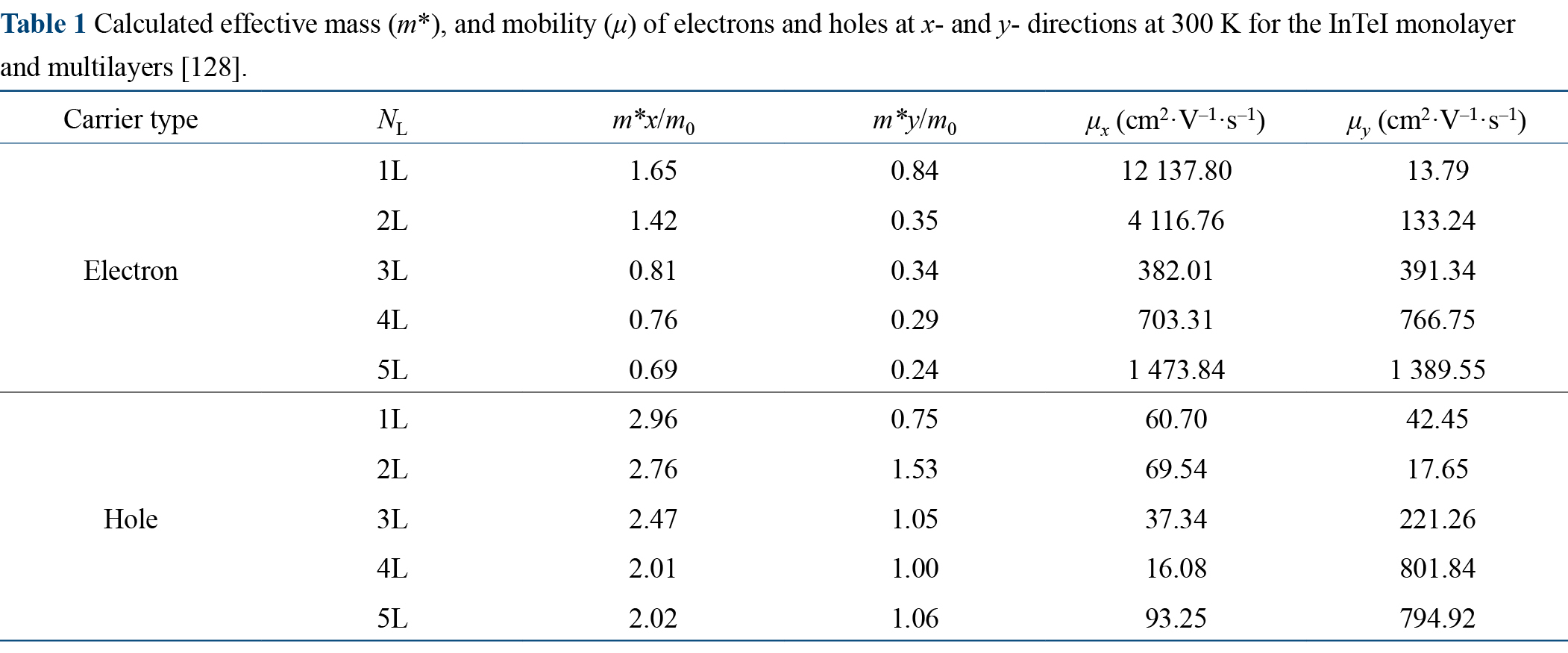
Jiang et al. show, based on first-principles calculations, that the new two-dimensional
material InTe has an extraordinary electron mobility: its x-direction electron mobility reaches 12 137.80 cm2·V–1·s–1, while the y-direction is only 13.79 cm2·V–1·s–1) (Table 1) [128].This remarkable mobility anisotropy gives InTe monolayers an advantage in nanoelectronic
devices. Combined with an intrinsic bandgap of 2.735 eV, the material is particularly
suitable for the construction of directional carrier transport channels in low-power,
high-frequency electronic devices. In particular, its low exfoliation energy of 0.21
J/m2 (only 52.5% of that of phosphene monolayers) provides a theoretical basis for realizing
mechanical exfoliation preparation of high-quality 2D structures, avoiding the defect
problems associated with complex chemical vapor deposition processes. Through systematic
strain engineering simulations, this work reveals a unique energy band modulation
law for InTe monolayers: the application of uniaxial strain induces a transition of
the material from an indirect to a direct bandgap. This tunable electronic structure
shows potential for applications in strain sensors and tunable optoelectronic devices.
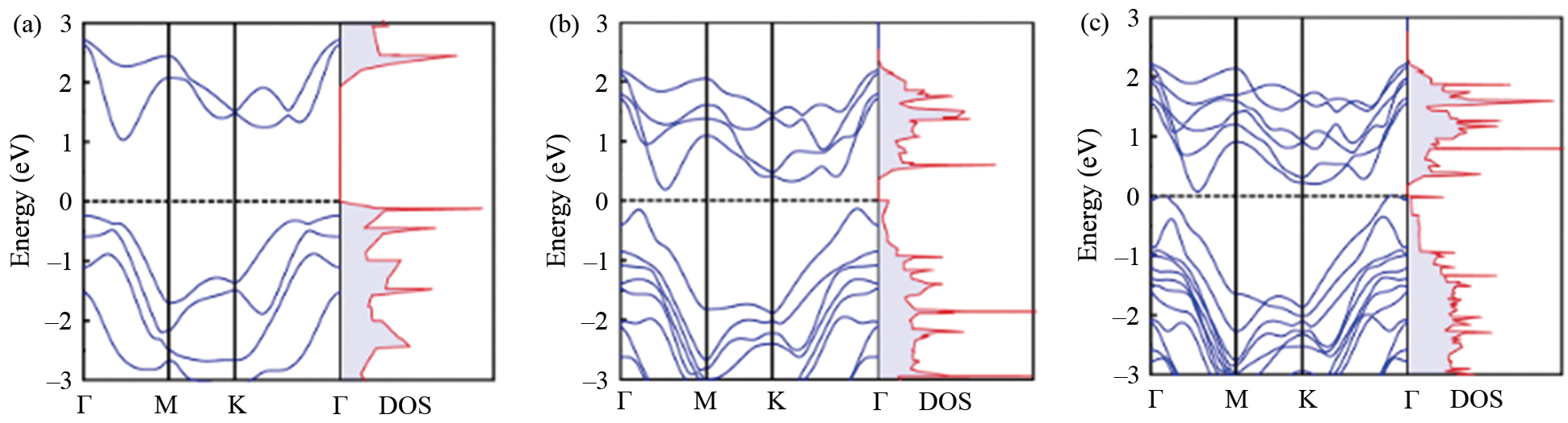
When extended to a multilayer structure, theoretical calculations show that the energy
bands of InTe form a quasi-direct bandgap feature near the gamma point, and this layer-dependent
energy band evolution law provides a new design dimension for the design of novel
stacked photodetectors. To address the environmental stability of 2D materials, the
ab initio molecular dynamics (AIMD) simulations of this work found that no dissociation
reaction occurred when gas-phase O2 interacted with InTe monolayers at room temperature, and the O2 dissociation energy barrier was calculated to be 0. The O2 dissociation energy barrier was calculated to be 0. 69 eV by the climbing image nudged
elastic band (CI-NEB) method, and its antioxidant performance is between that of black
phosphazene (0.31 eV) and α-P3Cl2 monolayer (1.14 eV), confirming that the material has the required environmental
stability for practical application. Notably, symmetry engineering strategies in 2D
transition metal systems have enabled reconfigurable p- and n-type FETs through structural
modulation, highlighting the critical role of crystal symmetry in carrier transport
optimization [129]. Further, recent advances further extend 2D materials to mid-infrared optoelectronics.
Yu et al. demonstrated that bilayer PtSe2 with controlled Se vacancies exhibits a tunable bandgap down to 0.3 eV (Fig. 11), enabling broadband photodetection from visible (632 nm) to mid-infrared (10 μm)
with responsivity up to 4.5 A·W–1 [130]. This defect engineering strategy, combined with the layer-dependent quantum confinement
effect, highlights the potential of 2D noble metal dichalcogenides to overcome the
traditional limitations of III–V and IV–VI semiconductors in long-wavelength photonic
integration.
Table 1 Calculated effective mass (
m*), and mobility (
μ) of electrons and holes at
x- and
y- directions at 300 K for the InTeI monolayer and multilayers [
128].
| Carrier type |
NL
|
m*x/m0 |
m*y/m0 |
μx (cm2·V–1·s–1) |
μy (cm2·V–1·s–1) |
|---|
| Electron |
1L |
1.65 |
0.84 |
12 137.80 |
13.79 |
| 2L |
1.42 |
0.35 |
4 116.76 |
133.24 |
| 3L |
0.81 |
0.34 |
382.01 |
391.34 |
| 4L |
0.76 |
0.29 |
703.31 |
766.75 |
| 5L |
0.69 |
0.24 |
1 473.84 |
1 389.55 |
| Hole |
1L |
2.96 |
0.75 |
60.70 |
42.45 |
| 2L |
2.76 |
1.53 |
69.54 |
17.65 |
| 3L |
2.47 |
1.05 |
37.34 |
221.26 |
| 4L |
2.01 |
1.00 |
16.08 |
801.84 |
| 5L |
2.02 |
1.06 |
93.25 |
794.92 |
Low-dimensional material systems (including two-dimensional, one-dimensional, and
zero-dimensional systems), as a frontier field of condensed matter physics and materials
science, have attracted much attention due to their unique physical properties and
potential for applications in microelectronic devices. Among them, one-dimensional
materials have become an important platform for the design of functional materials
due to their highly exposed active sites, significant aspect ratio features, and the
advantages of mechanical property modulation under dimensional constraints. Based
on this, Shen et al. present a novel one-dimensional PdGeS3 nanocrystalline chain system through first-principles calculations, which shows multidimensional
applications. Theoretical calculations show that the exfoliation energy of the material
is 105 meV/atom, which is lower than the solvation threshold for typical layered materials,
confirming that it can be prepared in a controlled manner by the mechanical exfoliation
method [131]. Phonon spectral analysis, together with AIMD simulation results, confirms the excellent
kinetic stability of the one-dimensional PdGeS3 nanocrystalline chains at room temperature. Electronic structure calculations show
that the material is an indirect bandgap semiconductor with a bandgap value of 2.86 eV
based on the HSE06 generalized correction and that effective modulation of the bandgap
value can be achieved by strain engineering. Notably, its electron mobility reaches
1506 cm2·V–1·s–1, which is 1–2 orders of magnitude higher than most of the reported one-dimensional
materials and some two-dimensional systems, while the hole mobility is only 18 cm2·V–1·s–1 (Table 2). This significant difference in carrier mobility is conducive to the realization
of highly efficient charge separation, which exhibits a unique advantage in the photocatalytic
field. Light absorption characterization shows that both single and multi-chain PdGeS3 exhibit strong absorption in the ultraviolet band with absorption coefficients in
the order of 10⁵ cm–1, which is highly compatible with their potential applications in field-effect transistors
and photodetectors. Through the synergistic application of multi-scale first-principle
computational methods, this study has constructed a complete theoretical framework
from structural stability, electronic properties, to photoresponse behavior, which
fully demonstrates the important role of computational material science in the design
and performance prediction of new low-dimensional materials.
Table 2 Calculated effective mass (|
m*|), and carrier mobility (
μ) of the electron and hole along the chain-directions at 300 K for the 1D PdGeS
3 nanochain [
131].
| System |
Carrier |
|m*| (m0) |
μ (cm2·V–1·s–1) |
|---|
| 1D PdGeS3 |
Hole |
3.88 |
18 |
| Electron |
0.53 |
1506 |
In the design of wide-bandgap semiconductor devices, material selection is crucial.
As the core foundation of device design, material selection requires accurate calculation
of intrinsic physical parameters such as electronic energy band structure, carrier
mobility, dielectric function, etc., to evaluate their technical applicability scientifically.
The first-principles calculations based on density functional theory can effectively
regulate key parameters such as forbidden bandwidth, carrier concentration, and lattice
thermal conductivity of materials, providing theoretical guidance for material system
optimization. Recent computational studies have expanded the horizon of unconventional
wide-gap semiconductors. For instance, Mg(OH)2—traditionally considered an insulator with a 5.7 eV bandgap—exhibits tunable conductivity
through impurity engineering. First-principles calculations reveal that trivalent
substitutional dopants (e.g., Al, Fe) introduce shallow donor states near the conduction
band, while interlayer F atoms act as shallow acceptors by creating hole states close
to the valence band maximum (Fig. 12) [132]. This dual doping mechanism demonstrates the feasibility of converting insulating
hydroxides into functional semiconductors through defect control. In the field of
optoelectronic device design, the DFT method can accurately predict optical parameters
such as exciton binding energy, optical absorption coefficient, and quantum efficiency
of materials, and reveal the structure-efficiency relationship between the microelectronic
structure of materials and the macro-optoelectronic performance. For device structure
optimization, the key factors such as interfacial state density, defect formation
energy, and carrier transport path can be systematically investigated by constructing
an atomic precision computational model, so as to establish a theoretical optimization
framework for device structure design. In addition, this technology can effectively
simulate the thermal transport behavior during device operation and guide the optimal
design of the thermal management system through phonon spectrum analysis and lattice
vibrational mode calculation. Finally, the overall performance of the device is subject
to the synergistic effect of multiple physical mechanisms: microscopic processes such
as carrier compound dynamics, interfacial energy band matching, and the point defect
evolution law all have a significant impact on the macroscopic properties of the device.
First-principles calculations can deeply analyze the interaction law of the above
complex physical mechanisms by establishing a multi-scale correlation model. It is
worth mentioning that this method can also simulate the structural degradation of
materials under continuous operation conditions, predict the failure mechanisms such
as oxygen vacancy migration and surface reconstruction, and provide a prospective
theoretical basis for device reliability research. Through the above discussion, it
is not difficult to obtain that the application of first-principles calculations in
the design of wide bandgap semiconductor devices has covered a variety of aspects,
such as material selection, structure optimization, performance prediction, etc.,
and has provided theoretical support for the efficient and stable operation of the
devices. With the continuous development of new technologies and methods, future research
will pay more attention to the combination of computation and experiment, as well
as the application of new computational methods. These innovations will promote the
further development of wide bandgap semiconductor device design and open up new research
areas and application directions.
4 Conclusion and outlook
First-principles calculations, as a core tool for revealing the physical nature of
wide bandgap semiconductors, have gradually evolved from static physical property
analysis to a comprehensive research paradigm of dynamic multiscale simulations. Through
the synergistic application of density functional theory, multibody perturbation theory,
and the Bethe-Salpeter equation, researchers have successfully achieved theoretical
breakthroughs ranging from the precise modification of electronic structure, the quantitative
analysis of exciton effects, and the cross-scale correlation of thermal transport
behavior. In the field of defect engineering, the doping strategy based on the calculation
of formation energy and migration barrier not only solves the problem of low efficiency
of traditional n-type doping but also promotes the breakdown field strength to break
through the 10 MV·cm–1 performance limit. In addition, the machine learning-learning high-throughput screening
technology has greatly accelerated the discovery process of novel semiconductor materials,
while the low-dimensional material design based on the first-principles calculations
has revealed a new mechanism of anisotropic carrier transport, which provides an entirely
new degree of freedom for the design of nanoelectronic devices.
However, the field still faces serious challenges. On the one hand, the limitation
of computational resources has become a bottleneck that limits the accurate simulation
of large-scale systems. Although hardware advances have significantly improved computational
efficiency, how to balance computational accuracy and scale is still the core contradiction
when dealing with complex electronic interaction systems. Second, the multi-scale
correlation mechanism between defects and interface effects has not been fully elucidated.
Although existing methods can simulate the behavior of a single defect, there are
still limitations in describing the dynamic evolution of defect clusters, interfacial
charge redistribution, and other complex processes, leading to systematic deviations
between theoretical predictions and experimental observations. Third, cross-scale
modeling of coupled optical-electrical-thermal multiphysical fields lacks a universal
framework, making it difficult to meet the demand for accurate prediction of device
performance under extreme conditions. Based on the above discussion, future research
needs to achieve a triple breakthrough at the methodological level:
(1) Develop efficient computational strategies enhanced by machine learning and optimize
the high-throughput screening process by active learning and migration learning.
(2) Establish a defect-interface co-evolutionary model by combining non-equilibrium
Green's function and real-time time-integrated density flooding theory to reveal the
temporal and spatial evolution of defect dynamics.
(3) To construct a cross-scale computational framework for multi-physics field coupling,
integrating electron-phonon interaction and non-adiabatic effects to realize a full
working condition simulation of device operation behavior.
It is expected that with the development of exascale supercomputing and quantum-classical
hybrid computing architectures, first-principles calculations will break through the
simulation limit of the multi-million atom system, and ultimately establish a cross-scale
correlation model from micro-defect regulation to macroscopic device performance,
which will provide theoretical cornerstones and design guides for the revolution of
wide-bandgap semiconductor technology.